MDEV-900-HP3-PPS-RS232 Linx Technologies Inc, MDEV-900-HP3-PPS-RS232 Datasheet - Page 2
MDEV-900-HP3-PPS-RS232
Manufacturer Part Number
MDEV-900-HP3-PPS-RS232
Description
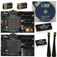
KIT MASTER 900MHZ HP-3 SIP RS232
Manufacturer
Linx Technologies Inc
Series
HP3r
Type
Receiverr
Datasheet
1.MDEV-900-HP3-PPS-RS232.pdf
(13 pages)
Specifications of MDEV-900-HP3-PPS-RS232
Frequency
902MHz ~ 928MHz
For Use With/related Products
HP3 Series RF Modules
Lead Free Status / RoHS Status
Contains lead / RoHS non-compliant
Other names
MDEV-900-HP3
MDEV-900-HP3
MDEV-900-HP3-PPS
MDEV-900-HP3-PPS
MDEV900HP3
MDEV900HP3PPSRS23
MDEV-900-HP3
MDEV-900-HP3-PPS
MDEV-900-HP3-PPS
MDEV900HP3
MDEV900HP3PPSRS23


Table 1: HP3 Series Receiver Specifications
Notes
1. Over the entire operating voltage range.
2. With the PDN pin low.
3. Serial mode.
4. Characterized, but not tested.
5. With 1kHz sine wave @ 115kHz transmitter deviation
6. No load.
7. With 1V output drop.
8. For 10
9. At specified center frequency.
Page 2
ELECTRICAL SPECIFICATIONS
Parameter
POWER SUPPLY
Operating Voltage
Supply Current
Power-Down Current
RECEIVE SECTION
Receive Frequency Range
Center Frequency Accuracy
Channel Spacing
First IF Frequency
Second IF Frequency
Noise Bandwidth
Data Rate
Analog / Audio Bandwidth
Analog / Audio Output Level
Data Output:
Output Impedance
Data Output Source Current
Receiver Sensitivity
RSSI:
Spurious Emissions
Interference Rejection:
ANTENNA PORT
RF Input Impedance
TIMING
Receiver Turn-On Time:
Channel Change Time
Max time between transitions
ENVIRONMENTAL
Operating Temperature Range
Logic Low
Logic High
via V
via PDN
Dynamic Range
Gain
Voltage With No Carrier
F C ±1MHz
F C ±5MHz
CC
-5
@ 9,600bps.
Designation
N
R
V
I
I
PDN
F
T4
T3
T2
T 1
CC
OUT
–
3DB
–
–
–
–
–
CC
C
V
902.62
CC
Min.
16.0
100
2.8
-50
0.8
0.0
-94
-30
50
60
–
–
–
–
–
–
–
–
–
–
–
–
–
–
–
–
–
-0.3
Typical
19.0
34.7
10.7
-100
250
280
230
3.0
5.6
1.1
-57
17
70
24
54
57
50
–
–
–
–
–
–
–
–
–
–
–
927.62
56,000
28,000
Max.
13.0
21.0
10.0
-107
+50
V
+85
2.0
0.5
1.6
7.0
3.0
1.5
80
20
–
–
–
–
–
–
–
–
–
–
–
CC
kohms
mV/dB
Units
mSec
mSec
mSec
mSec
VDC
MHz
MHz
MHz
VAC
VDC
VDC
dBm
dBm
kHz
kHz
kHz
mA
bps
µA
µA
Hz
dB
dB
dB
°
V
Ω
C
Notes
8,9
–
1
2
3
3
4
4
–
–
4
5
6
6
–
7
4
4
4
4
4
4
4
4
4
4
4
4
ABSOLUTE MAXIMUM RATINGS
PERFORMANCE DATA
TYPICAL PERFORMANCE GRAPHS
Figure 3: RX Enabled to Valid Data
Figure 5: Worst Case RSSI Response Time
1
2
CH1 1.00V
1
CH1 500mV
These performance parameters
are based on module operation at
25°C from a 3.0VDC supply unless
otherwise
illustrates
necessary
operation. It is recommended all
ground pins be connected to the
ground plane. The pins marked NC
have no electrical connection.
Supply Voltage V
Any Input or Output Pin
Operating Temperature
Storage Temperature
Soldering Temperature
*NOTE*
damage to the device. Furthermore, extended operation at these maximum
ratings may reduce the life of this device.
CH2 2.00V
PDN
Exceeding any of the limits of this section may lead to permanent
noted.
for
the
1mS
500uS
RX DATA
CC
testing
connections
Delta 4.080mS
Figure
Delta 1.920mS
and
2
Figure 2: Test / Basic Application Circuit
-0.3
-0.3
-30
-45
Figure 4: Receiver RSSI
Figure 6: BER vs. Input Power (typical)
BER
3.0
2.5
2.0
1.5
1.0
+260°C for 10 seconds
10
10
10
10
-110
-6
-5
-4
-3
-92 -93 -94 -95 -96 -97 -98 -99 -100 -101 -102
5VDC
PC
PC
PC
PC
-100
to
to
to
to
MODE
VCC
AUDIO
DATA
-90
ANT
GND
GND
GND
GND
GND
GND
GND
NC
CS0
CS1 / SS CLOCK
CS2 / SS DATA
PDN
RSSI
RF INPUT (dBm)
+18.0
-80
PIN (dBm)
V
+85
+85
CC
-70
NC
NC
NC
NC
NC
NC
NC
NC
NC
NC
NC
NC
NC
NC
NC
NC
NC
NC
-60
VDC
VDC
°C
°C
-50
Page 3
-40
Related parts for MDEV-900-HP3-PPS-RS232
Image
Part Number
Description
Manufacturer
Datasheet
Request
R

Part Number:
Description:
KIT MASTER 900MHZ HP-3 RS232 SMD
Manufacturer:
Linx Technologies Inc
Datasheet:

Part Number:
Description:
KIT MASTER 900MHZ HP-3 USB SMD
Manufacturer:
Linx Technologies Inc
Datasheet:

Part Number:
Description:
KIT MASTER 900MHZ HP-3 USB PIN
Manufacturer:
Linx Technologies Inc
Datasheet:

Part Number:
Description:
HOLDER BATTERY 20MM COIN CR2032
Manufacturer:
Linx Technologies Inc
Datasheet:

Part Number:
Description:
CONN RPSMA BL CRJA-CPV 8.5" COAX
Manufacturer:
Linx Technologies Inc

Part Number:
Description:
CABLE RG174 RPSMA M/F 8.5"
Manufacturer:
Linx Technologies Inc

Part Number:
Description:
CABLE RG174 SMA M/F 8.5"
Manufacturer:
Linx Technologies Inc

Part Number:
Description:
CABLE RPSMA/SMA 8.5"
Manufacturer:
Linx Technologies Inc

Part Number:
Description:
CABLE MALE-NMALE 8' RG-58 RPSMA
Manufacturer:
Linx Technologies Inc

Part Number:
Description:
CABLE RPSMA/SMA 8.5"
Manufacturer:
Linx Technologies Inc

Part Number:
Description:
MODULE USB LOW SPEED
Manufacturer:
Linx Technologies Inc
Datasheet:

Part Number:
Description:
IC TRANSCODER MT BI-DIR 20-SSOP
Manufacturer:
Linx Technologies Inc
Datasheet:

Part Number:
Description:
IC ENCODER LOW SECURITY 8DIP
Manufacturer:
Linx Technologies Inc
Datasheet:

Part Number:
Description:
IC DECODER MS SERIES 20-SSOP
Manufacturer:
Linx Technologies Inc
Datasheet:
Part Number:
Description:
IC ENCODER MS SERIES 20-SSOP
Manufacturer:
Linx Technologies Inc
Datasheet: