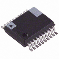
AD607ARSZ Analog Devices Inc, AD607ARSZ Datasheet

AD607ARSZ
Specifications of AD607ARSZ
Available stocks
Related parts for AD607ARSZ
AD607ARSZ Summary of contents
Page 1
FEATURES Complete Receiver-on-a-Chip: Monoceiver –15 dBm 1 dB Compression Point –8 dBm Input Third Order Intercept 500 MHz RF and LO Bandwidths Linear IF Amplifier Linear-in-dB Gain Control Manual Gain Control Quadrature Demodulator On-Board Phase-Locked Quadrature Oscillator Demodulates IFs ...
Page 2
AD607–SPECIFICATIONS Model DYNAMIC PERFORMANCE MIXER Maximum RF and LO Frequency Range Maximum Mixer Input Voltage Input 1 dB Compression Point Input Third-Order Intercept Noise Figure Maximum Output Voltage at MXOP Mixer Output Bandwidth at MXOP LO Drive Level LO Input ...
Page 3
ABSOLUTE MAXIMUM RATINGS Supply Voltage VPS1, VPS2 to COM1, COM2 . . . . . . . 5 Internal Power Dissipation . . . . . . . . . . . . . . . . ...
Page 4
AD607 Pin Mnemonic Reads 1 FDIN Frequency Detector Input 2 COM1 Common #1 3 PRUP Power-Up Input 4 LOIP Local Oscillator Input 5 RFLO RF “Low” Input 6 RFHI RF “High” Input 7 GREF Gain Reference Input 8 MXOP Mixer ...
Page 5
HP8656B IEEE RF_OUT SYNTHESIZER HP8656B RF_OUT IEEE 50 SYNTHESIZER HP8656B RF_OUT IEEE SYNTHESIZER HP6633A VPOS VNEG IEEE SPOS SNEG DCPS HP34401A HI CPIB LO I DMM R5 DP8200 1k VPOS VNEG IEEE HP8765B 0 SPOS SNEG 1 V REF ...
Page 6
AD607 HP346B 28V NOISE NOISE SOURCE HP6633A VPOS VNEG IEEE SPOS SNEG DCPS DP8200 VPOS VNEG IEEE SPOS SNEG V REF HP8764B 50 0 HP8656B IEEE RF_OUT SYNTHESIZER HP3326A DCFM OUTPUT_1 IEEE OUTPUT_2 ...
Page 7
HP6633A IEEE DP8200 IEEE HP34401A GPIB HP6633A IEEE DP8200 IEEE HP34401A GPIB HP3325B RF_OUT IEEE SYNTHESIZER HP6633A VPOS VNEG IEEE SPOS SNEG DCPS HP6633A VPOS VNEG IEEE SPOS SNEG DCPS HP34401A GPIB DMM REV. C VPOS VNEG SPOS SNEG DCPS ...
Page 8
AD607 FL6082A RF_OUT IEEE MOD_OUT HP6633A VPOS VNEG IEEE SPOS SNEG DCPS DP8200 VPOS VNEG IEEE SPOS SNEG V REF HP8112 PULSE_OUT IEEE PULSE GENERATOR HP8656B IEEE RF_OUT SYNTHESIZER HP6633A VPOS VNEG IEEE SPOS SNEG DCPS CHARACTERIZATION BOARD MXOP RFHI ...
Page 9
FL6082A RF_OUT IEEE MOD_OUT HP6633A VPOS VNEG IEEE SPOS SNEG DCPS DP8200 VPOS VNEG IEEE SPOS SNEG V REF HP3325B IEEE RF_OUT SYNTHESIZER HP3326 DCFM OUTPUT_1 IEEE OUTPUT_2 DUAL SYNTHESIZER HP6633A VPOS VNEG IEEE SPOS SNEG DCPS DP8200 VPOS VNEG ...
Page 10
AD607 VPOS C15 0.1 F GND C11 10nF FDIN R8 51.1 PRUP R7 LOIP 51.1 RFHI R6 51.1 R13 301 MXOP R14 * 54.9 332 IFHI 0.1 F *CONNECTIONS ARE DC-COUPLED. 4.99k R10 0.1 F C13 1 FDIN VPS1 0 ...
Page 11
VPOS = 5V 20MHz 15 VPOS = 3V 20MHz VPOS = 5V 10MHz VPOS = 3V 10MHz 110 130 ...
Page 12
AD607 0.3V GAIN 0.6V GAIN 1.2V GAIN 1.8V GAIN 2.4V GAIN 0 –10 0.1 1 INTERMEDIATE FREQUENCY – MHz TPC 7. IF ...
Page 13
IQ GAIN BALANCE – dB TPC 13. Demodulator Gain Balance, Histogram ° C, VPOS = 10.7 MHz I_GAIN_CORR 16 ...
Page 14
AD607 40.2127ms 40.2377ms TIMEBASE = 500 s/DIV DELAY MEMORY 1 = 100.0mV/DIV OFFSET TIMEBASE = 5.00 s/DIV DELAY MEMORY 2 = 60.00mV/DIV OFFSET TIMEBASE = 5.00 s/DIV DELAY DELTA T = 15.7990 s START = 40.2327ms STOP TRIGGER ON EXTERNAL ...
Page 15
The mixer’s RF input port is differential, that is, pin RFLO is functionally identical to RFHI, and these nodes are internally biased; we will generally assume that RFLO is decoupled to ac ground. The RF port can be modeled as ...
Page 16
AD607 The IF’s small-signal bandwidth is approximately 45 MHz from IFHI and IFLO through IFOP. The peak output at IFOP is ± 560 and ± 400 mV at the minimum V P 2.92 V. ...
Page 17
AD607 R T IFOP BPF DMIP a. Biasing DMIP from Power Supply (Assumes BPF AC-Coupled Internally) AD607 R T IFOP BPF DMIP VMID C BYPASS b. Biasing DMIP from VMID (Assumes BPF AC-Coupled Internally) Figure 19. Suggested Methods for Biasing ...
Page 18
AD607 Bias System The AD607 operates from a single supply typical supply current of 8 midgain and T = 27°C, corresponding to a power consumption of 25 mW. Any voltage from 2. 5.5 V ...
Page 19
As noted earlier, the gain reduced linearly with the voltage V on the GAIN pin. Figure 23 shows how the mixer and IF strip G gains vary with V when GREF is connected to VMID (1.5 V) ...
Page 20
AD607 VPOS GND FDIN PRUP C13 0 LO C14 0 RF C18 SHORT FDIN R14 C17 51.1 10nF VMID MOD FOR LARGE MAGNITUDE AC-COUPLED INPUT C15 JUMPER 0.1 F R10 R11 C11 4.99k OPEN 10nF C12 0 51.1 ...
Page 21
Figure 27b. Evaluation Board Layout, Bottom Side Table III. AD607 Evaluation Board Input and Output Connections Reference Connector Designation Type Description J1 SMA Frequency Detector Input J2 SMA Power-Up J3 SMA LO Input J4 SMA RF Input J5 SMA MGC ...
Page 22
AD607 In operation (Figure 28), the AD607 evaluation board draws about 8 midgain (59 dB). Use high impedance probes to monitor signals from the demodulated I and Q outputs and the IF output. The MGC voltage should be ...
Page 23
MIN COPLANARITY REV. C OUTLINE DIMENSIONS 20-Lead Shrink Small Outline Package [SSOP] (RS-20) Dimensions shown in millimeters 7.50 7.20 6. 8.20 5.60 7.80 5.30 7.40 5. 1.85 1.75 2.00 MAX 1.65 0.25 0.09 8 0.65 ...
Page 24
AD607 Revision History Location 11/02—Data Sheet changed from REV REV. C. Edits to SPECIFICATIONS . . . . . . . . . . . . . . . . . . . . . . . . ...


