ATA8204P3-TKQY Atmel, ATA8204P3-TKQY Datasheet - Page 13

ATA8204P3-TKQY
Manufacturer Part Number
ATA8204P3-TKQY
Description
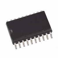
IC RCVR ASK/FSK UHF 433MHZ 20SSO
Manufacturer
Atmel
Datasheet
1.ATA8203P3-TKQY.pdf
(46 pages)
Specifications of ATA8204P3-TKQY
Frequency
433MHz
Sensitivity
-115dBm
Data Rate - Maximum
10 kbps
Modulation Or Protocol
ASK, FSK
Applications
General Purpose
Current - Receiving
8.5mA
Data Interface
PCB, Surface Mount
Antenna Connector
PCB, Surface Mount
Features
RSSI Equipped
Voltage - Supply
4.5 V ~ 5.5 V
Operating Temperature
-40°C ~ 85°C
Package / Case
20-SOIC (0.200", 5.30mm Width)
Pin Count
20
Screening Level
Industrial
Lead Free Status / RoHS Status
Lead free / RoHS Compliant
Memory Size
-
Lead Free Status / Rohs Status
Compliant
8.2
8.3
Figure 8-2.
9121B–INDCO–04/09
Data_out (DATA)
Bit-check Mode
Configuring the Bit Check
IC_ACTIVE
(Number of checked Bits: 3)
Bit check
Dem_out
Timing Diagram for Complete Successful Bit Check
Start-up mode
In bit-check mode the incoming data stream is examined to distinguish between a valid signal
from a corresponding transmitter and signals due to noise. This is done by subsequent time
frame checks where the distances between 2 signal edges are continuously compared to a pro-
grammable time window. The maximum number of these edge-to-edge tests, before the
receiver switches to receiving mode, is also programmable.
Assuming a modulation scheme that contains two edges per bit, two time frame checks verify
one bit. This is valid for Manchester, Bi-phase, and most other modulation schemes. The maxi-
mum count of bits to be checked can be set to 0, 3, 6, or 9 bits using the variable N
OPMODE register. This implies 0, 6, 12, and 18 edge-to-edge checks respectively. If N
set to a higher value, the receiver is less likely to switch to receiving mode due to noise. In the
presence of a valid transmitter signal, the bit check takes less time if N
value. In polling mode, the bit-check time is not dependent on NBit-check.
example where three bits are tested successfully and the data signal is transferred to pin DATA.
According to
If the edge-to-edge time t
bit-check limit T
the bit check is terminated and the receiver switches to sleep mode.
Figure 8-3.
T
Start-up
Figure
Valid Time Window for Bit Check
Lim_max
8-3, the time window for the bit check is defined by two separate time limits.
Dem_out
, the check continues. If t
1/2 Bit
ee
1/2 Bit
is in between the lower bit-check limit T
Start-check mode
T
Bit-check
1/2 Bit
T
T
Lim_max
Lim_min
ATA8203/ATA8204/ATA8205
Bit check ok
t
ee
1/2 Bit
ee
is smaller than T
1/f
Sig
1/2 Bit
1/2 Bit
Lim_min
Receiving mode
Bit-check
or t
Lim_min
Figure 8-2
ee
exceeds T
is set to a lower
and the upper
Bit-check
shows an
Bit-check
Lim_max
in the
13
is
,


