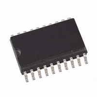
ATA8204P3-TKQY Atmel, ATA8204P3-TKQY Datasheet - Page 14

ATA8204P3-TKQY
Manufacturer Part Number
ATA8204P3-TKQY
Description
IC RCVR ASK/FSK UHF 433MHZ 20SSO
Manufacturer
Atmel
Datasheet
1.ATA8203P3-TKQY.pdf
(46 pages)
Specifications of ATA8204P3-TKQY
Frequency
433MHz
Sensitivity
-115dBm
Data Rate - Maximum
10 kbps
Modulation Or Protocol
ASK, FSK
Applications
General Purpose
Current - Receiving
8.5mA
Data Interface
PCB, Surface Mount
Antenna Connector
PCB, Surface Mount
Features
RSSI Equipped
Voltage - Supply
4.5 V ~ 5.5 V
Operating Temperature
-40°C ~ 85°C
Package / Case
20-SOIC (0.200", 5.30mm Width)
Pin Count
20
Screening Level
Industrial
Lead Free Status / RoHS Status
Lead free / RoHS Compliant
Memory Size
-
Lead Free Status / Rohs Status
Compliant
Figure 8-4.
14
(Lim_min = 14, Lim_max = 24)
IC_ACTIVE
Bit-check
Bit check
Dem_out
counter
ATA8203/ATA8204/ATA8205
Timing Diagram During Bit Check
Start-up mode
T
Start-up
For best noise immunity using a low span between T
achieved using a fixed frequency at a 50% duty cycle for the transmitter preburst. A “11111...” or
a “10101...” sequence in Manchester or Bi-phase is suitable for this. A good compromise
between receiver sensitivity and susceptibility to noise is a time window of ±30% regarding the
expected edge-to-edge time t
periods, the bit-check limits must be programmed according to the required span.
The bit-check limits are determined by means of the formula below.
T
T
Lim_min and Lim_max are defined by a 5-bit word each within the LIMIT register.
Using above formulas, Lim_min and Lim_max can be determined according to the required
T
mum edge-to-edge time t
“Digital Signal Processing” on page
imum value of the upper limit is Lim_max = 63.
If the calculated value for Lim_min is < 19, it is recommended to check 6 or 9 bits (N
prevent switching to receiving mode due to noise.
Figure
Lim_min = 14 and Lim_max = 24. When the IC is enabled, the signal processing circuits are
enabled during T
that period. When the bit check becomes active, the bit-check counter is clocked with the cycle
T
Figure 8-4
limits defined by Lim_min and Lim_max at the occurrence of a signal edge. In
check fails as the value CV_Lim is lower than the limit Lim_min. The bit check also fails if
CV_Lim reaches Lim_max. This is illustrated in
0
Lim_min
Lim_max
Lim_min
XClk
.
, T
= Lim_min
8-4,
1 2
= (Lim_max – 1)
Lim_max
shows how the bit check proceeds if the bit-check counter value CV_Lim is within the
3 4
Figure
T
5 6
XClk
Startup
and T
7 8
T
8-5, and
. The output of the ASK/FSK demodulator (Dem_out) is undefined during
1 2
XClk
XClk
3 4
. The time resolution defining T
ee
T
XClk
ee
(t
5 6
DATA_L_min
. Using pre-burst patterns that contain various edge-to-edge time
Figure 8-6
7 8
1/2 Bit
16. The lower limit should be set to Lim_min
9 10
Bit-check mode
11 12
, t
T
Bit-check
DATA_H_min
13 14
illustrate the bit check for the bit-check limits
Bit check ok
15 16
Figure
17 18
Lim_min
) is defined according to the
8-6.
1 2
Lim_min
3 4
and T
5 6
1/2 Bit
Lim_max
and T
7 8
9 10
Lim_max
is recommended. This is
11 12
Bit check ok
13 14
is T
Figure 8-5
15
9121B–INDCO–04/09
XClk
1 2
1/2 Bit
10. The max-
Section 8.6
. The mini-
3 4
Bit-check
the bit
) to


