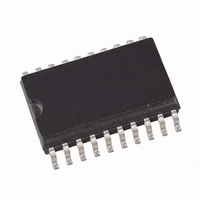
ATA8204P3-TKQY Atmel, ATA8204P3-TKQY Datasheet - Page 25

ATA8204P3-TKQY
Manufacturer Part Number
ATA8204P3-TKQY
Description
IC RCVR ASK/FSK UHF 433MHZ 20SSO
Manufacturer
Atmel
Datasheet
1.ATA8203P3-TKQY.pdf
(46 pages)
Specifications of ATA8204P3-TKQY
Frequency
433MHz
Sensitivity
-115dBm
Data Rate - Maximum
10 kbps
Modulation Or Protocol
ASK, FSK
Applications
General Purpose
Current - Receiving
8.5mA
Data Interface
PCB, Surface Mount
Antenna Connector
PCB, Surface Mount
Features
RSSI Equipped
Voltage - Supply
4.5 V ~ 5.5 V
Operating Temperature
-40°C ~ 85°C
Package / Case
20-SOIC (0.200", 5.30mm Width)
Pin Count
20
Screening Level
Industrial
Lead Free Status / RoHS Status
Lead free / RoHS Compliant
Memory Size
-
Lead Free Status / Rohs Status
Compliant
11. Configuring the Receiver
Table 11-3.
9121B–INDCO–04/09
Bit 1
1
0
0
values of
Bit 3...14
values of
Bit 3...14
Default
Default
–
–
Bit 2
–
1
0
Effect of the Configuration Words within the Registers
Baud1
Bit 3
Lim_
min5
–
0
0
BR_Range
Baud0
Bit 4
Lim_
min4
–
0
1
The ATA8203/ATA8204/ATA8205 receiver is configured using two 12-bit RAM registers called
OPMODE and LIMIT. The registers can be programmed by means of the bidirectional DATA
port. If the register content has changed due to a voltage drop, this condition is indicated by a
the output pattern called reset marker (RM). If this occurs, the receiver must be reprogrammed.
After a Power-On Reset (POR), the registers are set to default mode. If the receiver is operated
in default mode, there is no need to program the registers.
structure of the registers. According to
to polling mode using the OFF command (see
programmed. Bit 2 represents the register address. It selects the appropriate register to be pro-
grammed. For high programming reliability, bit 15 (Stop bit), at the end of the programming
operation, must be set to 0.
Table 11-1.
Table 11-2.
Bit 1
BitChk1
1
0
0
Bit 5
Lim_
min3
–
0
0
Lim_min
N
Bit 15
Bit-check
0
1
Effect of Bit 1 and Bit 2 on Programming the Registers
Effect of Bit 15 on Programming the Register
BitChk0
Bit 6
Lim_
min2
–
1
1
Bit 2
x
1
0
Modu-
_FSK
lation
ASK/
Bit 7
Lim_
min1
–
0
0
Action
The receiver is set back to polling mode (OFF command)
The OPMODE register is programmed
The LIMIT register is programmed
Action
The values are written into the register (OPMODE or LIMIT)
The values are not written into the register
OFF command
OPMODE register
Sleep4
Bit 8
Lim_
min0
LIMIT register
–
0
1
Sleep3
Table
max5
Bit 9
Lim_
–
0
1
ATA8203/ATA8204/ATA8205
11-1, bit 1 defines whether the receiver is set back
Sleep2
Bit 10
max4
Lim_
Sleep
“Receiving Mode” on page
–
1
0
Sleep1
Bit 11
max3
Lim_
–
1
1
Lim_max
Table 11-3 on page 25
Sleep0 X
Bit 12
max2
Lim_
–
0
0
Bit 13
X
max1
SleepStd
Lim_
Sleep
–
0
0
15) or whether it is
Suppression
Disable
Noise_
Bit 14
Noise
max0
Lim_
–
1
1
shows the
Bit 15
–
–
0
–
–
–
0
–
25


