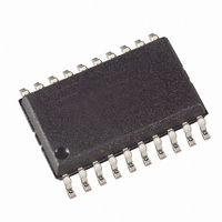
ATA5743P3-TGQY Atmel, ATA5743P3-TGQY Datasheet - Page 19

ATA5743P3-TGQY
Manufacturer Part Number
ATA5743P3-TGQY
Description
IC RCVR ASK/FSK 300KHZ 20SOIC
Manufacturer
Atmel
Datasheet
1.ATA5743P3-TGQY.pdf
(43 pages)
Specifications of ATA5743P3-TGQY
Frequency
300MHz ~ 450MHz
Sensitivity
-110dBm
Data Rate - Maximum
10 kBaud
Modulation Or Protocol
ASK, FSK
Applications
RKE, Telemetering, Security Technology
Current - Receiving
7.5mA
Data Interface
PCB, Surface Mount
Antenna Connector
PCB, Surface Mount
Voltage - Supply
4.5 V ~ 5.5 V
Operating Temperature
-40°C ~ 105°C
Package / Case
20-SOIC (0.300", 7.50mm Width)
Operating Frequency (max)
450000kHz
Operating Temperature (min)
-40C
Operating Temperature (max)
105C
Operating Temperature Classification
Industrial
Operating Supply Voltage (min)
4.5V
Operating Supply Voltage (typ)
5V
Operating Supply Voltage (max)
5.5V
Lead Free Status / RoHS Status
Lead free / RoHS Compliant
Features
-
Memory Size
-
Lead Free Status / Rohs Status
Compliant
Available stocks
Company
Part Number
Manufacturer
Quantity
Price
Company:
Part Number:
ATA5743P3-TGQY
Manufacturer:
ATMEL
Quantity:
203
Part Number:
ATA5743P3-TGQY
Manufacturer:
ATMEL/爱特梅尔
Quantity:
20 000
Figure 6-13. Activating the Receiving Mode via Pin POLLING/_ON
6.4
6.4.1
4839B–RKE–08/05
Data Clock
Generation of the Data Clock
IC_ACTIVE
POLLING/_ON
Data_out (DATA)
Serial bi-directional
data line
Figure 6-12 on page 18
POLLING/_ON. The pin POLLING/_ON must be held to low for the time period t
positive edge on pin POLLING/_ON and the delay t
time T
This command is faster than using pin DATA, but at the cost of an additional connection to the
microcontroller.
Figure 6-13
pin POLLING/_ON must be held to Low. After the delay t
mode to start-up mode regardless of the programmed values for T
POLLING/_ON is held to Low, the values for T
(see section
If the receiver is polled exclusively by a microcontroller, T
(permanent sleep mode). In this case, the receiver remains in sleep mode as long as POLL-
ING/_ON is held to High.
The pin DATA_CLK makes a data shift clock available to sample the data stream into a shift
register. Using this data clock, a microcontroller can easily synchronize the data stream. This
clock can only be used for Manchester- and Bi-phase-coded signals.
After a successful bit check, the receiver switches from polling mode to receiving mode and the
data stream is available at pin DATA. In receiving mode, the data clock control logic (Manches-
ter/Bi-phase demodulator) is active and examines the incoming data stream. This is done, as in
the bit check, by subsequent time frame checks where the distance between two edges is con-
tinuously compared to a programmable time window. As illustrated in
only two distances between two edges in Manchester- and Bi-phase-coded signals are valid
(T and 2T).
The limits for T are the same as used for the bit check. They can be programmed in the
LIMIT-register (Lim_min and Lim_max, see
Sleep
elapses.
Sleep mode
illustrates how to set the receiver to receive mode via the pin POLLING/_ON. The
“Digital Noise Suppression” on page
illustrates how to set the receiver back to polling mode via pin
t
on1
Start-up mode
Table 6-10 on page 27
Sleep
22).
and N
on3
, the polling mode is active and the sleep
Bit-check
on1
, the receiver changes from sleep
Sleep
Receiving mode
will be ignored, but not deleted
Sleep
X
X
must be programmed to 31
and
Figure 6-14 on page
and N
Table 6-11 on page
Bit-check
ATA5743
on2
. As long as
. After the
27).
20,
19


