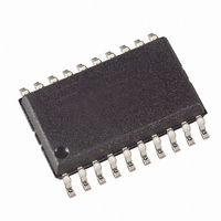
ATA5743P6-TGQY Atmel, ATA5743P6-TGQY Datasheet - Page 22

ATA5743P6-TGQY
Manufacturer Part Number
ATA5743P6-TGQY
Description
IC RCVR ASK/FSK 600KHZ 20SOIC
Manufacturer
Atmel
Datasheet
1.ATA5743P3-TGQY.pdf
(43 pages)
Specifications of ATA5743P6-TGQY
Frequency
300MHz ~ 450MHz
Sensitivity
-110dBm
Data Rate - Maximum
10 kBaud
Modulation Or Protocol
ASK, FSK
Applications
RKE, Telemetering, Security Technology
Current - Receiving
7.5mA
Data Interface
PCB, Surface Mount
Antenna Connector
PCB, Surface Mount
Voltage - Supply
4.5 V ~ 5.5 V
Operating Temperature
-40°C ~ 105°C
Package / Case
20-SOIC (0.300", 7.50mm Width)
Operating Frequency (max)
450000kHz
Operating Temperature (min)
-40C
Operating Temperature (max)
105C
Operating Temperature Classification
Industrial
Operating Supply Voltage (min)
4.5V
Operating Supply Voltage (typ)
5V
Operating Supply Voltage (max)
5.5V
Lead Free Status / RoHS Status
Lead free / RoHS Compliant
Features
-
Memory Size
-
Lead Free Status / Rohs Status
Compliant
Available stocks
Company
Part Number
Manufacturer
Quantity
Price
Company:
Part Number:
ATA5743P6-TGQY
Manufacturer:
ATMEL
Quantity:
222
Part Number:
ATA5743P6-TGQY
Manufacturer:
ATMEL/爱特梅尔
Quantity:
20 000
6.5
6.5.1
22
Digital Noise Suppression
ATA5743
Automatic Noise Suppression
Figure 6-18. Timing Characteristic of the Data Clock (Rising Edge on Pin DATA)
Figure 6-19. Timing Characteristic of the Data Clock (Falling Edge on Pin DATA)
After a data transmission, digital noise appears on the data output (see
To prevent digital noise from keeping the connected microcontroller busy, it can be suppressed
in two different ways.
The automatic noise suppression is illustrated in
Noise_Disable
receiver changes to bit-check mode at the end of a valid data stream. The digital noise is sup-
pressed and the level at pin DATA is High in that case. The receiver changes back to receiving
mode, if the bit check was successful.
This way of suppressing the noise is recommended if the data stream is Manchester or Bi-phase
coded and is active after power on.
Figure 6-22 on page 23
Note that if the last period of the data stream is a high period (rising edge to falling edge), a
pulse occurs on pin DATA. The length of the pulse depends on the selected baud-rate range.
Serial bi-directional
data line
Data_In
DATA_CLK
Data_Out
Serial bi-directional
data line
Data_In
DATA_CLK
(Table 6-9 on page
Data_Out
illustrates the behavior of the data output at the end of a data stream.
V
V
Ih
II
= 0.35
= 0.65
V
26) in the OPMODE register is set to “1” (default), the
V
V
X
S
S
t
Delay1
t
Delay
t
Delay1
t
Delay
t
Delay2
t
P_Data_Clk
t
Delay2
t
P_Data_Clk
V
V
Figure 6-21 on page
V
X
Ih
II
= 0.35
= 0.65
V
V
S
S
Figure 6-20 on page
23. If the bit
4839B–RKE–08/05
23).


