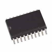
ATA5724P3-TKQY Atmel, ATA5724P3-TKQY Datasheet - Page 15

ATA5724P3-TKQY
Manufacturer Part Number
ATA5724P3-TKQY
Description
IC RCVR ASK/FSK UHF 20-SSOP
Manufacturer
Atmel
Datasheet
1.ATA5723-DK.pdf
(46 pages)
Specifications of ATA5724P3-TKQY
Frequency
433MHz
Sensitivity
-113dBm
Data Rate - Maximum
10 kbps
Modulation Or Protocol
ASK, FSK
Applications
General Purpose
Current - Receiving
11mA
Data Interface
PCB, Surface Mount
Antenna Connector
PCB, Surface Mount
Voltage - Supply
4.5 V ~ 5.5 V
Operating Temperature
-40°C ~ 125°C
Package / Case
20-SOIC (0.200", 5.30mm Width)
Operating Temperature (min)
-40C
Operating Temperature (max)
105C
Operating Temperature Classification
Industrial
Product Depth (mm)
4.4mm
Operating Supply Voltage (min)
4.5V
Operating Supply Voltage (typ)
5V
Operating Supply Voltage (max)
5.5V
Lead Free Status / RoHS Status
Lead free / RoHS Compliant
Features
-
Memory Size
-
Lead Free Status / Rohs Status
Compliant
Available stocks
Company
Part Number
Manufacturer
Quantity
Price
Part Number:
ATA5724P3-TKQY
Manufacturer:
ATMEL/爱特梅尔
Quantity:
20 000
Figure 8-5.
Figure 8-6.
8.4
8.5
9106E–RKE–07/08
Duration of the Bit Check
Receiving Mode
(Lim_min = 14, Lim_max = 24)
(Lim_min = 14, Lim_max = 24)
IC_ACTIVE
IC_ACTIVE
Bit-check
Bit-check
Bit check
Dem_out
Bit check
Dem_out
counter
counter
Timing Diagram for Failed Bit Check (Condition: CV_Lim < Lim_min)
Timing Diagram for Failed Bit Check (Condition: CV_Lim
Start-up mode
Start-up mode
T
T
Start-up
Start-up
If no transmitter signal is present during the bit check, the output of the ASK/FSK demodulator
delivers random signals. The bit check is a statistical process and T
Therefore, an average value for T
depends on the selected baud-rate range and on T
value for T
In the presence of a valid transmitter signal, T
nal, f
a longer period for T
If the bit check was successful for all bits specified by N
mode. According to
that case, and the data clock is available after the start bit has been detected (see
page
the data clock at pin DATA_CLK. The receiver stays in that condition until it is switched back to
polling mode explicitly.
0
0
Sig
20). A connected microcontroller can be woken up by the negative edge at pin DATA or by
, and the count of the checked bits, N
1 2
1 2
Bit-check
3 4
3 4
5 6
5 6
resulting in a lower current consumption in polling mode.
1
7 1
Bit-check mode
Bit-check
Figure 8-2 on page
2 3
T
Bit-check
2 3
4 5
Bit check failed (CV_Lim_ < Lim_min)
4 5
1/2 Bit
requiring a higher value for the transmitter pre-burst T
6 7
Bit-check mode
6 7
8
T
Bit-check
8
9 10
9 10
Bit-check
11 12
1/2 Bit
11 12
13, the internal data signal is switched to pin DATA in
ATA5723/ATA5724/ATA5728
13 14
is given in the electrical characteristics. T
Bit-check
15 16
Bit-check
Lim_max)
Bit check failed (CV_Lim
17 18
. A higher value for N
Clk
Sleep mode
19 20
. A higher baud-rate range causes a lower
is dependent on the frequency of that sig-
T
Sleep
Bit-check
0
21 22
23 24
, the receiver switches to receiving
Bit-check
Lim_max)
Sleep mode
Bit-check
T
varies for each check.
Sleep
0
thereby results in
Preburst
Figure 9-1 on
.
Bit-check
15


