ATA5724P3-TKQY Atmel, ATA5724P3-TKQY Datasheet - Page 19

ATA5724P3-TKQY
Manufacturer Part Number
ATA5724P3-TKQY
Description
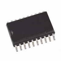
IC RCVR ASK/FSK UHF 20-SSOP
Manufacturer
Atmel
Datasheet
1.ATA5723-DK.pdf
(46 pages)
Specifications of ATA5724P3-TKQY
Frequency
433MHz
Sensitivity
-113dBm
Data Rate - Maximum
10 kbps
Modulation Or Protocol
ASK, FSK
Applications
General Purpose
Current - Receiving
11mA
Data Interface
PCB, Surface Mount
Antenna Connector
PCB, Surface Mount
Voltage - Supply
4.5 V ~ 5.5 V
Operating Temperature
-40°C ~ 125°C
Package / Case
20-SOIC (0.200", 5.30mm Width)
Operating Temperature (min)
-40C
Operating Temperature (max)
105C
Operating Temperature Classification
Industrial
Product Depth (mm)
4.4mm
Operating Supply Voltage (min)
4.5V
Operating Supply Voltage (typ)
5V
Operating Supply Voltage (max)
5.5V
Lead Free Status / RoHS Status
Lead free / RoHS Compliant
Features
-
Memory Size
-
Lead Free Status / Rohs Status
Compliant
Available stocks
Company
Part Number
Manufacturer
Quantity
Price
Part Number:
ATA5724P3-TKQY
Manufacturer:
ATMEL/爱特梅尔
Quantity:
20 000
9. Data Clock
9.1
9106E–RKE–07/08
Generation of the Data Clock
Figure 8-11
set the receiver back to polling mode using pin POLLING/_ON. The pin POLLING/_ON must be
held to low for the time period t
t
Using the POLLING/_ON command is faster than using pin DATA; however, this requires the
use of an additional connection to the microcontroller.
Figure 8-12
receiver to receiving mode using the pin POLLING/_ON. The pin POLLING/_ON must be held to
low. After the delay t
the programmed values for T
ues for T
Suppression” on page
If the receiver is polled exclusively by a microcontroller, T
manent sleep mode). In this case the receiver remains in sleep mode as long as POLLING/_ON
is held to high.
The pin DATA_CLK makes a data shift clock available to sample the data stream into a shift reg-
ister. Using this data clock, a microcontroller can easily synchronize the data stream. This clock
can only be used for Manchester and Bi-phase coded signals.
After a successful bit check, the receiver switches from polling mode to receiving mode and the
data stream is available at pin DATA. In receiving mode, the data clock control logic (Man-
chester/Bi-phase demodulator) is active and examines the incoming data stream. This is done,
as with the bit check, by subsequent time frame checks where the distance between two edges
is continuously compared to a programmable time window. As illustrated in
20, only two distances between two edges in Manchester and Bi-phase coded signals are valid
(T and 2T).
The limits for T are the same as used with the bit check. They can be programmed in the
LIMIT-register (Lim_min and Lim_max, see
28).
The limits for 2T are calculated as follows:
Lower limit of 2T:
Upper limit of 2T:
(If the result for ’Lim_min_2T’ or ’Lim_max_2T’ is not an integer value, it is rounded up.)
The data clock is available, after the data clock control logic has detected the distance 2T (Start
bit) and is issued with the delay t
If the data clock control logic detects a timing or logical error (Manchester code violation), as
illustrated in
clock. The receiver remains in receiving mode and starts with the bit check. If the bit check was
successful and the start bit has been detected, the data clock control logic starts again with the
generation of the data clock (see
on3
, the polling mode is active and the sleep time T
Sleep
“Timing Diagram of the OFF Command using Pin POLLING/_ON” illustrates how to
“Activating the Receiving Mode using Pin “POLLING/_ON” illustrates how to set the
Figure 9-2 on page 20
and N
on1
Bit-check
23).
Lim_min_2T = (Lim_min + Lim_max) – (Lim_max – Lim_min)/2
Lim_max_2T= (Lim_min + Lim_max) + (Lim_max – Lim_min)/2
, the receiver changes from sleep mode to start-up mode regardless of
Sleep
is ignored, but not deleted (see
on2
Delay
Figure 9-4 on page
and N
. After the positive edge on pin POLLING/_ON and the delay
and
after the edge on pin DATA (see
Bit-check
Figure 9-3 on page
ATA5723/ATA5724/ATA5728
Table 11-10 on page 28
. As long as POLLING/_ON is held to low, the val-
Sleep
21).
elapses.
Sleep
21, it stops the output of the data
must be programmed to 31 (per-
Section 10. “Digital Noise
and
Figure 9-1 on page
Table 11-11 on page
Figure 9-1 on page
20).
19


