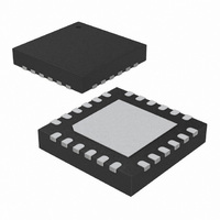
ATA5746-PXQW Atmel, ATA5746-PXQW Datasheet - Page 17

ATA5746-PXQW
Manufacturer Part Number
ATA5746-PXQW
Description
IC RCVR ASK/FSK UHF 24-QFN
Manufacturer
Atmel
Datasheet
1.ATA5745-EK.pdf
(44 pages)
Specifications of ATA5746-PXQW
Frequency
315MHz
Sensitivity
-114dBm
Data Rate - Maximum
10 kbps
Modulation Or Protocol
ASK, FSK
Applications
Alarm and Security Systems, RKE, TPMS
Current - Receiving
6.7mA
Data Interface
PCB, Surface Mount
Antenna Connector
PCB, Surface Mount
Voltage - Supply
2.7 V ~ 3.3 V, 4.5 V ~ 5.5 V
Operating Temperature
-40°C ~ 105°C
Package / Case
24-VQFN Exposed Pad, 24-HVQFN, 24-SQFN, 24-DHVQFN
Lead Free Status / RoHS Status
Lead free / RoHS Compliant
Features
-
Memory Size
-
Available stocks
Company
Part Number
Manufacturer
Quantity
Price
Company:
Part Number:
ATA5746-PXQW
Manufacturer:
ATMEL
Quantity:
3
3.1
3.2
4596B–RKE–06/07
Pin CLK_OUT
Basic Clock Cycle of the Digital Circuitry
Pin CLK_OUT is an output to clock a connected microcontroller. The clock is available in
Standby and Active modes. The frequency f
CLK_OUT_CTRL0 and CLK_OUT_CTRL1, and is calculated as follows:
Table 3-2.
The signal at CLK_OUT output has a nominal 50% duty cycle. To save current, it is recom-
mended that CLK_OUT be switched off during Standby mode.
The complete timing of the digital circuitry is derived from one clock. As seen in
page
divider.
T
- Debouncing of the data signal stream
- Start-up time of the RX signal path
The start-up time and the debounce characteristic depend on the selected bit rate range
(BR_Range) which is defined by pins BR0 and BR1. The clock cycle T
lowing formulas for further reference:
BR_Range
f
DCLK
DCLK
CLK_OUT_CTRL1
16, this clock cycle, T
=
controls the following application relevant parameters:
f
---------- -
XTO
16
0
0
1
1
Setting of f
CLK_OUT_CTRL0
CLK_OUT
DCLK
, is derived from the crystal oscillator (XTO) in combination with a
0
1
0
1
ATA5745/ATA5746 [Preliminary]
BR_Range 0: T
BR_Range 1: T
BR_Range 2: T
BR_Range 3: T
C L K _ O U T
Clock on pin CLK_OUT is switched off
XDCLK
XDCLK
XDCLK
XDCLK
(Low level on pin CLK_OUT)
= 8
= 4
= 2
= 1
can be adjusted via the pins
f
f
f
CLK_OUT
CLK_OUT
CLK_OUT
Function
T
T
T
T
DCLK
DCLK
DCLK
DCLK
= f
XDCLK
= f
= f
XTO
XTO
XTO
/ 12
is defined by the fol-
/ 3
/ 6
Figure 3-2 on
17


