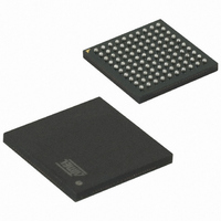
ATMEGA256RZBV-8CU Atmel, ATMEGA256RZBV-8CU Datasheet - Page 4

ATMEGA256RZBV-8CU
Manufacturer Part Number
ATMEGA256RZBV-8CU
Description
BUNDLE ATMEGA2560V/AT86RF230-ZU
Manufacturer
Atmel
Series
ATMEGAr
Datasheet
1.ATMEGA64RZAPV-10MU.pdf
(21 pages)
Specifications of ATMEGA256RZBV-8CU
Frequency
2.4GHz
Modulation Or Protocol
802.15.4 Zigbee
Applications
ISM, ZigBee™
Power - Output
3dBm
Sensitivity
-101dBm
Voltage - Supply
1.8 V ~ 3.6 V
Current - Receiving
15.5mA
Current - Transmitting
16.5mA
Data Interface
PCB, Surface Mount
Memory Size
256kB Flash, 4kB EEPROM, 8kB RAM
Antenna Connector
PCB, Surface Mount
Package / Case
100-TFBGA
Wireless Frequency
2.4 GHz
Interface Type
SPI, USART
Output Power
3 dBm
For Use With
ATAVRISP2 - PROGRAMMER AVR IN SYSTEMATJTAGICE2 - AVR ON-CHIP D-BUG SYSTEM
Lead Free Status / RoHS Status
Lead free / RoHS Compliant
Operating Temperature
-
Data Rate - Maximum
-
Lead Free Status / Rohs Status
Lead free / RoHS Compliant
For Use With/related Products
ATmega256
3.3 Description of Power and Filter Circuit
3.4 Description of STK500 Interface
4
AVR414
• Better tolerance to less than perfect RF ground.
However, the RZ502 has a typical single ended SMA stub antenna mounted. A
special circuit is required to convert the 100Ω differential RF input/output pins of the
AT86RF230 to a 50Ω single ended RF port. This is solved by a BALUN circuit on the
RZ502 top module. A BALUN (a compound term meaning “BAlanced-UNbalanced”) is
a passive component that transforms impedance. Two capacitors are added as a DC
block. Figure 3-2 depicts the BALUN circuit described above.
Figure 3-2 BALUN Circuit
Figure 3-3 shows the power and filter circuit connected to the AT86RF230. The power
circuit is built from three components; a SMD fuse (F1), a Zener diode (D1) and a
jumper (JP1). D1 is a 3.9 Volts Zener diode connected in series with the thermal fuse.
This connection prevents excessive voltages on the DVTG (Digital Voltage) and
AVTG (Analog Voltage) ports when JP1 is closed, and potentially harm the
AT86RF230. JP1 can also be used for current measurements.
The rightmost part of Figure 3-3 is a PI-type LC (two shunt capacitors and one series
inductor) filter used to suppress noise and harmonics to enter the analog/RF part of
the radio transceiver.
Figure 3-3 Power and Filter Circuit
The STK500 board has two expansion connectors, one on each side of the
programming module. All AVR I/O ports, programming signals and control signals are
routed to these connectors. Figure 3-4 depicts the pin-out of expansion connector 1.
This connector is used by the RZ502 top module to mount itself to the
STK500/STK501 board stack. And ultimately connect the AT86RF230 radio
RFN
RFP
C1
C2
Balanced 1
Balanced 2
BALUN
Unbalanced
SMA Connector
8051A-AVR-11/06


