MRF24WB0MA/RM Microchip Technology, MRF24WB0MA/RM Datasheet - Page 15
MRF24WB0MA/RM
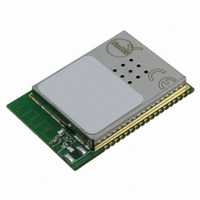
Manufacturer Part Number
MRF24WB0MA/RM
Description
TXRX RF 2.4GHZ PCB ANT 802.11B
Manufacturer
Microchip Technology
Specifications of MRF24WB0MA/RM
Frequency
2.4GHz
Data Rate - Maximum
1Mbps
Modulation Or Protocol
802.11 b
Applications
ISM
Power - Output
10dBm
Sensitivity
-91dBm
Voltage - Supply
2.7 V ~ 3.6 V
Current - Receiving
85mA
Current - Transmitting
154mA
Data Interface
PCB, Surface Mount
Antenna Connector
On-Board, Trace
Operating Temperature
0°C ~ 70°C
Package / Case
Module
Wireless Frequency
2.4 GHz
Interface Type
SPI, JTAG
Board Size
21 mm x 31 mm
Modulation
DSSS
Security
WEP, WPA-PSK, WPA-2-PSK
Operating Voltage
2.7 V to 3.6 V
Antenna
PCB Meander
Operating Temperature Range
0 C to + 70 C
Frequency Rf
2.4GHz
Transmit Power
9mW
Module Interface
SPI, 4-Wire
Modulation Type
DSSS
Data Rate Max
2Mbps
Supply Current
154mA
Supply Voltage Range
2.7V To 3.6V
Frequency Range
2.4GHz
Leaded Process Compatible
Yes
Rohs Compliant
Yes
For Use With/related Products
PIC18, PIC24, dsPIC33, PIC32
Lead Free Status / RoHS Status
Lead free / RoHS Compliant
Memory Size
-
Lead Free Status / Rohs Status
Lead free / RoHS Compliant
Available stocks
Company
Part Number
Manufacturer
Quantity
Price
Company:

Part Number:
MRF24WB0MA/RM
Manufacturer:
MICROCHIP
Quantity:
2 000


2.3.4
The Standby state is not user-controlled but is noted as
it helps identify and track certain operations of the
module during power tracing.
TABLE 2-1:
FIGURE 2-3:
2.4
Joint Test Action Group (JTAG) is the common name
used for the IEEE 1149.1 standard entitled Standard
Test Access Port and Boundary-Scan Architecture for
test access ports that are used for testing printed circuit
boards using boundary scan. The MRF24WB0MA/
MRF24WB0MB supports JTAG boundary scan. The
JTAG port provides the optional hardware JTAG Reset
input, JTAG
driven high to enable JTAG mode. JTAG should not be
enabled during normal functional operation. This func-
tion affects power state current.
2010 Microchip Technology Inc.
Hibernate
Standby
RX ON
TX ON
Sleep
State
Off
Note 1: See Section 2.2.
JTAG Interface
Hibernate
STANDBY STATE
RST
. JTAG_EN and JTAG
MRF24WB0MA/MRF24WB0MB POWER STATE DEFINITIONS
VDD
3.3V
3.3V
3.3V
3.3V
3.3V
MRF24WB0MA/MRF24WB0MB POWER-STATE DIAGRAM
0V
Note 1
Off
MRF24WB0MA/MRF24WB0MB
3.3V
RST
CS
0V
0V
0V
0V
0V
need to be
Standby
Note 1
Description
Power is completely disconnected
All internal power regulators are OFF – enabled by HIBERNATE pin
Enabled by TCPIP driver
Receive circuits are on and receiving
Transmit circuits are on and transmitting
State machine transition state only – not user controlled
2.5
The MRF24WB0MA/MRF24WB0MB incorporates a
Transmitted Data pin (DEBUG
pin (DEBUG
pins can be connected to commercially available RS-
232 line drivers/receivers with appropriate external
level shifters. The serial interface is fully tested at
115200 bits/seconds with RS-232/UART interface
applications.
RX On
200 us
Sleep
200 us
Debug Serial Interface
RX
) for serial debugging purposes. These
10 us
TX
) and a Received Data
TX On
DS70632A-page 15
Related parts for MRF24WB0MA/RM
Image
Part Number
Description
Manufacturer
Datasheet
Request
R

Part Number:
Description:
Manufacturer:
Microchip Technology Inc.
Datasheet:
Part Number:
Description:
Manufacturer:
Microchip Technology Inc.
Datasheet:
Part Number:
Description:
Manufacturer:
Microchip Technology Inc.
Datasheet:
Part Number:
Description:
Manufacturer:
Microchip Technology Inc.
Datasheet:
Part Number:
Description:
Manufacturer:
Microchip Technology Inc.
Datasheet:
Part Number:
Description:
Manufacturer:
Microchip Technology Inc.
Datasheet:
Part Number:
Description:
Manufacturer:
Microchip Technology Inc.
Datasheet:
Part Number:
Description:
Manufacturer:
Microchip Technology Inc.
Datasheet: