MRF24WB0MA/RM Microchip Technology, MRF24WB0MA/RM Datasheet - Page 9
MRF24WB0MA/RM
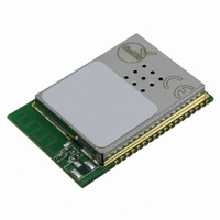
Manufacturer Part Number
MRF24WB0MA/RM
Description
TXRX RF 2.4GHZ PCB ANT 802.11B
Manufacturer
Microchip Technology
Specifications of MRF24WB0MA/RM
Frequency
2.4GHz
Data Rate - Maximum
1Mbps
Modulation Or Protocol
802.11 b
Applications
ISM
Power - Output
10dBm
Sensitivity
-91dBm
Voltage - Supply
2.7 V ~ 3.6 V
Current - Receiving
85mA
Current - Transmitting
154mA
Data Interface
PCB, Surface Mount
Antenna Connector
On-Board, Trace
Operating Temperature
0°C ~ 70°C
Package / Case
Module
Wireless Frequency
2.4 GHz
Interface Type
SPI, JTAG
Board Size
21 mm x 31 mm
Modulation
DSSS
Security
WEP, WPA-PSK, WPA-2-PSK
Operating Voltage
2.7 V to 3.6 V
Antenna
PCB Meander
Operating Temperature Range
0 C to + 70 C
Frequency Rf
2.4GHz
Transmit Power
9mW
Module Interface
SPI, 4-Wire
Modulation Type
DSSS
Data Rate Max
2Mbps
Supply Current
154mA
Supply Voltage Range
2.7V To 3.6V
Frequency Range
2.4GHz
Leaded Process Compatible
Yes
Rohs Compliant
Yes
For Use With/related Products
PIC18, PIC24, dsPIC33, PIC32
Lead Free Status / RoHS Status
Lead free / RoHS Compliant
Memory Size
-
Lead Free Status / Rohs Status
Lead free / RoHS Compliant
Available stocks
Company
Part Number
Manufacturer
Quantity
Price
Company:

Part Number:
MRF24WB0MA/RM
Manufacturer:
MICROCHIP
Quantity:
2 000


TABLE 1-1:
2010 Microchip Technology Inc.
Legend: Pin type abbreviation: P = Power input, I = Input, O = Output, NC = Do Not Connect
Note 1:
Pin
10
12
13
14
15
16
17
18
19
20
21
22
23
24
25
26
27
28
29
30
31
32
33
34
35
36
11
1
2
3
4
5
6
7
8
9
2:
Signals of Type “I: Constant” must either be constantly driven by the host or have a pull-up or pull-down (in
case the host is likely to tri-state the signal during power down modes). The constant drive is used to
ensure defined operation of the part and to minimize leakage current during low power modes.
WP is used as write-protect for the internal module SPI Flash. For production use, this pin should be
pulled low. For end application, this pin can be controlled by the host microcontroller to enable in field
Flash updates.
HIBERNATE
DEBUG
DEBUG
JTAG
JTAG
JTAG
JTAG
JTAG
Symbol
JTAG
RESET
Pin Description
WP
GND
GND
GND
GND
GND
GND
GND
GND
VDD
VDD
SDO
SCK
SDI
INT
NC
NC
NC
NC
NC
NC
NC
NC
CS
NC
NC
(2)
TDO
TCK
TMS
RST
TDI
EN
RX
TX
I: Constant
I: Constant
Type
NC
NC
NC
NC
NC
NC
NC
NC
NC
NC
MRF24WB0MA/MRF24WB0MB
P
O
P
P
P
P
P
O
P
P
P
O
O
P
I
I
I
I
I
I
I
I
I
I
(1)
(1)
Description
Ground
Do not connect
JTAG test data output
JTAG clock input
JTAG mode input
JTAG test data input
Module Reset input
Do not connect
JTAG Reset input (optional; see Section 2.0)
Ground
Do not connect
Do not connect
Do not connect
Do not connect
Do not connect
Write protect (this pin is used to enable FLASH update)
Power
Ground
Ground
Hibernate mode enable (high input will disable the module)
JTAG test enable
Do not connect
SPI Chip Select input
Do not connect
Ground
Serial debug port input (see Section 2.0)
Serial debug port output (see Section 2.0)
Ground
Power
Ground
Do not connect
SPI data out
Interrupt output (open drain – requires a pull-up)
SPI clock input
SPI data in
Ground
Preliminary
DS70632A-page 9
Related parts for MRF24WB0MA/RM
Image
Part Number
Description
Manufacturer
Datasheet
Request
R

Part Number:
Description:
Manufacturer:
Microchip Technology Inc.
Datasheet:
Part Number:
Description:
Manufacturer:
Microchip Technology Inc.
Datasheet:
Part Number:
Description:
Manufacturer:
Microchip Technology Inc.
Datasheet:
Part Number:
Description:
Manufacturer:
Microchip Technology Inc.
Datasheet:
Part Number:
Description:
Manufacturer:
Microchip Technology Inc.
Datasheet:
Part Number:
Description:
Manufacturer:
Microchip Technology Inc.
Datasheet:
Part Number:
Description:
Manufacturer:
Microchip Technology Inc.
Datasheet:
Part Number:
Description:
Manufacturer:
Microchip Technology Inc.
Datasheet: