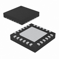
ATA5773-PXQW Atmel, ATA5773-PXQW Datasheet - Page 116

ATA5773-PXQW
Manufacturer Part Number
ATA5773-PXQW
Description
XMITTR UHF ASK/FSK 310MHZ 24VQFN
Manufacturer
Atmel
Datasheet
1.ATA5773-DK1.pdf
(219 pages)
Specifications of ATA5773-PXQW
Frequency
310MHz ~ 350MHz
Modulation Or Protocol
UHF
Power - Output
8dBm
Voltage - Supply
2 V ~ 4 V
Current - Transmitting
9.8mA
Data Interface
PCB, Surface Mount
Memory Size
4kB Flash, 256B EEPROM, 256B SRAM
Antenna Connector
PCB, Surface Mount
Operating Temperature
-40°C ~ 85°C
Package / Case
24-VQFN Exposed Pad, 24-HVQFN, 24-SQFN, 24-DHVQFN
Processor Series
ATA5x
Core
AVR8
Data Bus Width
8 bit
Program Memory Type
Flash
Program Memory Size
4 KB
Data Ram Size
256 B
Interface Type
SPI, USI
Maximum Clock Frequency
4 MHz
Number Of Programmable I/os
12
Number Of Timers
2
Maximum Operating Temperature
+ 85 C
Mounting Style
SMD/SMT
Minimum Operating Temperature
- 40 C
On-chip Adc
10 bit, 12 Channel
Lead Free Status / RoHS Status
Lead free / RoHS Compliant
Applications
-
Sensitivity
-
Data Rate - Maximum
-
Current - Receiving
-
Lead Free Status / Rohs Status
Details
Available stocks
Company
Part Number
Manufacturer
Quantity
Price
Company:
Part Number:
ATA5773-PXQW
Manufacturer:
ATMEL
Quantity:
3 500
Part Number:
ATA5773-PXQW
Manufacturer:
ATMEL/爱特梅尔
Quantity:
20 000
- Current page: 116 of 219
- Download datasheet (4Mb)
4.16.11
4.16.11.1
116
Atmel ATA5771/73/74
Register Description
TCCR1A – Timer/Counter1 Control Register A
• Bit 7:6 – COM1A1:0: Compare Output Mode for Channel A
• Bit 5:4 – COM1B1:0: Compare Output Mode for Channel B
The COM1A1:0 and COM1B1:0 control the Output Compare pins (OC1A and OC1B respec-
tively) behavior. If one or both of the COM1A1:0 bits are written to one, the OC1A output
overrides the normal port functionality of the I/O pin it is connected to. If one or both of the
COM1B1:0 bit are written to one, the OC1B output overrides the normal port functionality of
the I/O pin it is connected to. However, note that the Data Direction Register (DDR) bit corre-
sponding to the OC1A or OC1B pin must be set in order to enable the output driver.
When the OC1A or OC1B is connected to the pin, the function of the COM1x1:0 bits is depen-
dent of the WGM13:0 bits setting.
WGM13:0 bits are set to a Normal or a CTC mode (non-PWM).
Table 4-39.
Table 4-40
PWM mode.
Table 4-40.
Note:
Bit
0x2F (0x4F)
Read/Write
Initial Value
COM1A1/COM1B1
COM1A1/COM1B1
1. A special case occurs when OCR1A/OCR1B equals TOP and COM1A1/COM1B1 is set. In
0
0
1
1
0
0
1
1
this case the compare match is ignored, but the set or clear is done at BOTTOM.
4.15.7.3 “Fast PWM Mode” on page 83
shows the COM1x1:0 bit functionality when the WGM13:0 bits are set to the fast
COM1A1
Compare Output Mode, non-PWM
Compare Output Mode, Fast PWM
R/W
7
0
COM1A0
COM1A0/COM1B0
COM1A0/COM1B0
R/W
6
0
0
1
0
1
0
1
0
1
COM1B1
R/W
Table 4-39
5
0
COM1B0
R/W
4
0
Description
Normal port operation, OC1A/OC1B disconnected.
Toggle OC1A/OC1B on Compare Match.
Clear OC1A/OC1B on Compare Match (Set output to
low level).
Set OC1A/OC1B on Compare Match (Set output to
high level).
Description
Normal port operation, OC1A/OC1B disconnected.
WGM13=0: Normal port operation, OC1A/OC1B
disconnected.
WGM13=1: Toggle OC1A on Compare Match, OC1B
reserved.
Clear OC1A/OC1B on Compare Match, set
OC1A/OC1B at BOTTOM (non-inverting mode)
Set OC1A/OC1B on Compare Match, clear
OC1A/OC1B at BOTTOM (inverting mode)
shows the COM1x1:0 bit functionality when the
for more details.
(1)
R
3
0
–
R
2
–
0
WGM11
R/W
1
0
WGM10
R/W
0
0
9137E–RKE–12/10
Section
TCCR1A
Related parts for ATA5773-PXQW
Image
Part Number
Description
Manufacturer
Datasheet
Request
R

Part Number:
Description:
BOARD XMITTER FOR ATA5773 315MHZ
Manufacturer:
Atmel
Datasheet:

Part Number:
Description:
Microcontroller With Uhf Ask/fsk Transmitter
Manufacturer:
ATMEL Corporation
Datasheet:

Part Number:
Description:
DEV KIT FOR AVR/AVR32
Manufacturer:
Atmel
Datasheet:

Part Number:
Description:
INTERVAL AND WIPE/WASH WIPER CONTROL IC WITH DELAY
Manufacturer:
ATMEL Corporation
Datasheet:

Part Number:
Description:
Low-Voltage Voice-Switched IC for Hands-Free Operation
Manufacturer:
ATMEL Corporation
Datasheet:

Part Number:
Description:
MONOLITHIC INTEGRATED FEATUREPHONE CIRCUIT
Manufacturer:
ATMEL Corporation
Datasheet:

Part Number:
Description:
AM-FM Receiver IC U4255BM-M
Manufacturer:
ATMEL Corporation
Datasheet:

Part Number:
Description:
Monolithic Integrated Feature Phone Circuit
Manufacturer:
ATMEL Corporation
Datasheet:

Part Number:
Description:
Multistandard Video-IF and Quasi Parallel Sound Processing
Manufacturer:
ATMEL Corporation
Datasheet:

Part Number:
Description:
High-performance EE PLD
Manufacturer:
ATMEL Corporation
Datasheet:

Part Number:
Description:
8-bit Flash Microcontroller
Manufacturer:
ATMEL Corporation
Datasheet:

Part Number:
Description:
2-Wire Serial EEPROM
Manufacturer:
ATMEL Corporation
Datasheet:


