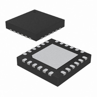
ATA5771-PXQW Atmel, ATA5771-PXQW Datasheet - Page 190

ATA5771-PXQW
Manufacturer Part Number
ATA5771-PXQW
Description
XMITTR UHF ASK/FSK 868MHZ 24VQFN
Manufacturer
Atmel
Datasheet
1.ATA5773-DK1.pdf
(219 pages)
Specifications of ATA5771-PXQW
Frequency
868MHz ~ 928MHz
Modulation Or Protocol
UHF
Power - Output
8dBm
Voltage - Supply
2 V ~ 4 V
Current - Transmitting
9.8mA
Data Interface
PCB, Surface Mount
Memory Size
4kB Flash, 256B EEPROM, 256B SRAM
Antenna Connector
PCB, Surface Mount
Operating Temperature
-40°C ~ 85°C
Package / Case
24-VQFN Exposed Pad, 24-HVQFN, 24-SQFN, 24-DHVQFN
Processor Series
ATA5x
Core
AVR8
Data Bus Width
8 bit
Program Memory Type
Flash
Program Memory Size
4 KB
Data Ram Size
256 B
Interface Type
SPI, USI
Maximum Clock Frequency
4 MHz
Number Of Programmable I/os
12
Number Of Timers
2
Maximum Operating Temperature
+ 85 C
Mounting Style
SMD/SMT
Minimum Operating Temperature
- 40 C
On-chip Adc
10 bit, 12 Channel
Lead Free Status / RoHS Status
Lead free / RoHS Compliant
Applications
-
Sensitivity
-
Data Rate - Maximum
-
Current - Receiving
-
Lead Free Status / Rohs Status
Details
Available stocks
Company
Part Number
Manufacturer
Quantity
Price
Company:
Part Number:
ATA5771-PXQW
Manufacturer:
ATMEL
Quantity:
218
- Current page: 190 of 219
- Download datasheet (4Mb)
8.3.3.3
8.3.4
Table 8-3.
Notes:
Table 8-4.
190
*) Type means: A = 100% tested, C = Characterized on samples
Note:
Symbol
V
V
RAM
t
V
t
I
HYST
BOD
BG
BG
BG
1. Values are guidelines only.
2. This is the limit to which VDD can be lowered without losing RAM data
(2)
1. V
Atmel ATA5771/73/74
BODLEVEL
System and Reset Characterizations
is tested down to V
drops to a voltage where correct operation of the microcontroller is no longer guaranteed
External Clock Drive
BOT
111
110
001
000
010
011
101
Reset, Brown-out and Internal Voltage Reference Characteristics
Parameter
Brown-out Detector Hysteresis
RAM Retention Voltage
Min Pulse Width on Brown-out Reset
Bandgap reference voltage
Bandgap reference start-up time
Bandgap reference current consumption
BODLEVEL Fuse Coding
may be below nominal minimum operating voltage for some devices. For devices where this is the case, the device
Table 8-2.
Symbol
1/t
t
t
t
t
t
CLCL
CHCX
CLCX
CLCH
CHCL
CC
t
CLCL
CLCL
= V
(1)
BOT
Min V
during the production test. This guarantees that a Brown-out Reset will occur before V
Parameter
Clock Frequency
Clock Period
High Time
Low Time
Rise Time
Fall Time
Change in period from one clock cycle to the next
(1)
1.7
1.7
1.8
2.0
2.1
2.5
External Clock Drive
BOT
Typ V
1.8
1.9
2.0
2.2
2.3
2.7
V
V
V
C C
C C
C C
BOD Disabled
BOT
= 2.7V, T
= 2.7V, T
= 2.7V, T
Condition
A
A
A
= 25°C
= 25°C
= 25°C
Max V
(1)
2.0
2.1
2.2
2.4
2.5
2.9
BOT
Min
1.0
50
Min.
100
40
40
V
0
CC
Typ
100
= 2.7 - 3.6V
1.1
40
10
2
Unit
V
Max.
1.6
1.6
10
2
Max
250
1.2
70
9137E–RKE–12/10
Type*
A
C
C
C
C
A
MHz
Unit
Unit
mV
mV
µA
ns
µs
ns
ns
ns
µs
µs
CC
%
V
Related parts for ATA5771-PXQW
Image
Part Number
Description
Manufacturer
Datasheet
Request
R

Part Number:
Description:
BOARD XMITTER FOR ATA5771 868MHZ
Manufacturer:
Atmel
Datasheet:

Part Number:
Description:
Manufacturer:
ATMEL Corporation
Datasheet:

Part Number:
Description:
DEV KIT FOR AVR/AVR32
Manufacturer:
Atmel
Datasheet:

Part Number:
Description:
INTERVAL AND WIPE/WASH WIPER CONTROL IC WITH DELAY
Manufacturer:
ATMEL Corporation
Datasheet:

Part Number:
Description:
Low-Voltage Voice-Switched IC for Hands-Free Operation
Manufacturer:
ATMEL Corporation
Datasheet:

Part Number:
Description:
MONOLITHIC INTEGRATED FEATUREPHONE CIRCUIT
Manufacturer:
ATMEL Corporation
Datasheet:

Part Number:
Description:
AM-FM Receiver IC U4255BM-M
Manufacturer:
ATMEL Corporation
Datasheet:

Part Number:
Description:
Monolithic Integrated Feature Phone Circuit
Manufacturer:
ATMEL Corporation
Datasheet:

Part Number:
Description:
Multistandard Video-IF and Quasi Parallel Sound Processing
Manufacturer:
ATMEL Corporation
Datasheet:

Part Number:
Description:
High-performance EE PLD
Manufacturer:
ATMEL Corporation
Datasheet:

Part Number:
Description:
8-bit Flash Microcontroller
Manufacturer:
ATMEL Corporation
Datasheet:

Part Number:
Description:
2-Wire Serial EEPROM
Manufacturer:
ATMEL Corporation
Datasheet:


