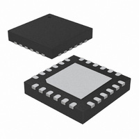
ATA5771-PXQW Atmel, ATA5771-PXQW Datasheet - Page 24

ATA5771-PXQW
Manufacturer Part Number
ATA5771-PXQW
Description
XMITTR UHF ASK/FSK 868MHZ 24VQFN
Manufacturer
Atmel
Datasheet
1.ATA5773-DK1.pdf
(219 pages)
Specifications of ATA5771-PXQW
Frequency
868MHz ~ 928MHz
Modulation Or Protocol
UHF
Power - Output
8dBm
Voltage - Supply
2 V ~ 4 V
Current - Transmitting
9.8mA
Data Interface
PCB, Surface Mount
Memory Size
4kB Flash, 256B EEPROM, 256B SRAM
Antenna Connector
PCB, Surface Mount
Operating Temperature
-40°C ~ 85°C
Package / Case
24-VQFN Exposed Pad, 24-HVQFN, 24-SQFN, 24-DHVQFN
Processor Series
ATA5x
Core
AVR8
Data Bus Width
8 bit
Program Memory Type
Flash
Program Memory Size
4 KB
Data Ram Size
256 B
Interface Type
SPI, USI
Maximum Clock Frequency
4 MHz
Number Of Programmable I/os
12
Number Of Timers
2
Maximum Operating Temperature
+ 85 C
Mounting Style
SMD/SMT
Minimum Operating Temperature
- 40 C
On-chip Adc
10 bit, 12 Channel
Lead Free Status / RoHS Status
Lead free / RoHS Compliant
Applications
-
Sensitivity
-
Data Rate - Maximum
-
Current - Receiving
-
Lead Free Status / Rohs Status
Details
Available stocks
Company
Part Number
Manufacturer
Quantity
Price
Company:
Part Number:
ATA5771-PXQW
Manufacturer:
ATMEL
Quantity:
218
- Current page: 24 of 219
- Download datasheet (4Mb)
4.8.3
4.8.3.1
4.8.3.2
4.8.3.3
4.8.3.4
24
Atmel ATA5771/73/74
EEPROM Data Memory
EEPROM Read/Write Access
Atomic Byte Programming
Split Byte Programming
Erase
The Atmel
arate data space, in which single bytes can be read and written. The EEPROM has an
endurance of at least 100,000 write/erase cycles. The access between the EEPROM and the
CPU is described in the following, specifying the EEPROM Address Registers, the EEPROM
Data Register, and the EEPROM Control Register. For a detailed description of Serial data
downloading to the EEPROM, see
The EEPROM Access Registers are accessible in the I/O space.
The write access times for the EEPROM are given in
tion, however, lets the user software detect when the next byte can be written. If the user code
contains instructions that write the EEPROM, some precautions must be taken. In heavily
filtered power supplies, V
device for some period of time to run at a voltage lower than specified as minimum for the
clock frequency used. See
details on how to avoid problems in these situations.
In order to prevent unintentional EEPROM writes, a specific write procedure must be followed.
See
Programming” on page 24
When the EEPROM is read, the CPU is halted for four clock cycles before the next instruction
is executed. When the EEPROM is written, the CPU is halted for two clock cycles before the
next instruction is executed.
Using Atomic Byte Programming is the simplest mode. When writing a byte to the EEPROM,
the user must write the address into the EEARL Register and data into EEDR Register. If the
EEPMn bits are zero, writing EEPE (within four cycles after EEMPE is written) will trigger the
erase/write operation. Both the erase and write cycle are done in one operation and the total
programming time is given in Table 1. The EEPE bit remains set until the erase and write
operations are completed. While the device is busy with programming, it is not possible to do
any other EEPROM operations.
It is possible to split the erase and write cycle in two different operations. This may be useful if
the system requires short access time for some limited period of time (typically if the power
supply voltage falls). In order to take advantage of this method, it is required that the locations
to be written have been erased before the write operation. But since the erase and write oper-
ations are split, it is possible to do the erase operations when the system allows doing
time-critical operations (typically after Power-up).
To erase a byte, the address must be written to EEAR. If the EEPMn bits are 0b01, writing the
EEPE (within four cycles after EEMPE is written) will trigger the erase operation only (pro-
gramming time is given in Table 1). The EEPE bit remains set until the erase operation
completes. While the device is busy programming, it is not possible to do any other EEPROM
operations.
Section 4.8.3.2 “Atomic Byte Programming” on page 24
®
ATtiny44V contains 256 bytes of data EEPROM memory. It is organized as a sep-
CC
for details on this.
Section 4.8.3.6 “Preventing EEPROM Corruption” on page 27
is likely to rise or fall slowly on Power-up/down. This causes the
Section 4.23.6 “Serial Downloading” on page
Table 4-2 on page
and
Section 4.8.3.3 “Split Byte
30. A self-timing func-
9137E–RKE–12/10
169.
for
Related parts for ATA5771-PXQW
Image
Part Number
Description
Manufacturer
Datasheet
Request
R

Part Number:
Description:
BOARD XMITTER FOR ATA5771 868MHZ
Manufacturer:
Atmel
Datasheet:

Part Number:
Description:
Manufacturer:
ATMEL Corporation
Datasheet:

Part Number:
Description:
DEV KIT FOR AVR/AVR32
Manufacturer:
Atmel
Datasheet:

Part Number:
Description:
INTERVAL AND WIPE/WASH WIPER CONTROL IC WITH DELAY
Manufacturer:
ATMEL Corporation
Datasheet:

Part Number:
Description:
Low-Voltage Voice-Switched IC for Hands-Free Operation
Manufacturer:
ATMEL Corporation
Datasheet:

Part Number:
Description:
MONOLITHIC INTEGRATED FEATUREPHONE CIRCUIT
Manufacturer:
ATMEL Corporation
Datasheet:

Part Number:
Description:
AM-FM Receiver IC U4255BM-M
Manufacturer:
ATMEL Corporation
Datasheet:

Part Number:
Description:
Monolithic Integrated Feature Phone Circuit
Manufacturer:
ATMEL Corporation
Datasheet:

Part Number:
Description:
Multistandard Video-IF and Quasi Parallel Sound Processing
Manufacturer:
ATMEL Corporation
Datasheet:

Part Number:
Description:
High-performance EE PLD
Manufacturer:
ATMEL Corporation
Datasheet:

Part Number:
Description:
8-bit Flash Microcontroller
Manufacturer:
ATMEL Corporation
Datasheet:

Part Number:
Description:
2-Wire Serial EEPROM
Manufacturer:
ATMEL Corporation
Datasheet:


