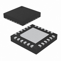
ATA8742-PXQW Atmel, ATA8742-PXQW Datasheet - Page 165

ATA8742-PXQW
Manufacturer Part Number
ATA8742-PXQW
Description
MCU W/TRANSMITTER ASK/FSK 24QFN
Manufacturer
Atmel
Datasheet
1.ATA8742-PXQW.pdf
(238 pages)
Specifications of ATA8742-PXQW
Frequency
433MHz
Applications
Home Automation, Remote Sensing, RKE
Modulation Or Protocol
ASK, FSK
Data Rate - Maximum
32 kBit/s
Power - Output
7.5dBm
Current - Transmitting
9.8mA
Data Interface
PCB, Surface Mount
Antenna Connector
PCB, Surface Mount
Memory Size
4kB Flash, 256B EEPROM, 256B SRAM
Voltage - Supply
2 V ~ 4 V
Operating Temperature
-40°C ~ 85°C
Package / Case
24-VQFN Exposed Pad, 24-HVQFN, 24-SQFN, 24-DHVQFN
Processor Series
ATA8x
Core
AVR8
Data Bus Width
8 bit
Program Memory Type
Flash
Program Memory Size
4 KB
Data Ram Size
256 B
Interface Type
SPI, USI
Maximum Clock Frequency
8.1 MHz
Number Of Programmable I/os
12
Number Of Timers
2
Maximum Operating Temperature
+ 85 C
Mounting Style
SMD/SMT
Development Tools By Supplier
ATASTK512-EK1-IND
Minimum Operating Temperature
- 40 C
On-chip Adc
10 bit, 8 Channel
Lead Free Status / RoHS Status
Lead free / RoHS Compliant
Features
-
Lead Free Status / Rohs Status
Details
Available stocks
Company
Part Number
Manufacturer
Quantity
Price
Company:
Part Number:
ATA8742-PXQW
Manufacturer:
ATMEL
Quantity:
1 482
- Current page: 165 of 238
- Download datasheet (4Mb)
25.8.3
25.9
Table 25-2.
9151A–INDCO–07/09
Temperature / °C
Voltage / mV
Temperature Measurement
Bipolar Differential Conversion
Temperature vs. Sensor Output Voltage (Typical Case)
than the voltage of the negative pin or otherwise the voltage difference is saturated to zero. The
result is presented in one-sided form, from 0x000 (0d) through 0x3FF (+1023d). The GAIN is
either 1x or 20x.
If differential channels and a bipolar input mode are used, the result is
where V
and V
0x200 (-512d) through 0x1FF (+511d). The GAIN is either 1x or 20x. Note that if the user wants
to perform a quick polarity check of the result, it is sufficient to read the MSB of the result (ADC9
in ADCH). If the bit is one, the result is negative, and if this bit is zero, the result is positive.
As default the ADC converter operates in the unipolar input mode, but the bipolar input mode
can be selected by writing the BIN bit in the ADCSRB to one. In the bipolar input mode two-sided
voltage differences are allowed and thus the voltage on the negative input pin can also be larger
than the voltage on the positive input pin.
The temperature measurement is based on an on-chip temperature sensor that is coupled to a
single ended ADC8 channel. Selecting the ADC8 channel by writing the MUX5:0 bits in ADMUX
register to “100010” enables the temperature sensor. The internal 1.1V reference must also be
selected for the ADC reference source in the temperature sensor measurement. When the tem-
perature sensor is enabled, the ADC converter can be used in single conversion mode to
measure the voltage over the temperature sensor. The measured voltage has a linear relation-
ship to the temperature as described in Table 51. The voltage sensitivity is approximately 1 mV /
°
gap is always calibrated and its accuracy is only guaranteed between 1.0V and 1.2V
The values described in
variation the temperature sensor output voltage varies from one chip to another. To be capable
of achieving more accurate results the temperature measurement can be calibrated in the appli-
cation software. The software calibration requires that a calibration value is measured and
stored in a register or EEPROM for each chip, as a part of the production test. The software cal-
ibration can be done utilizing the formula:
where ADCn are the ADC data registers, k is a fixed coefficient and T
sor offset value determined and stored into EEPROM as a part of the production test.To obtain
best accuracy the coefficient k should be measured using two temperature calibrations. Using
offset calibration, set k = 1.0, where k = (1024*1.07mV/°C)/1.1V~1.0 [1/°C].
C and the accuracy of the temperature measurement is +/-
REF
243 mV
-40°C
POS
the selected voltage reference. The result is presented in two’s complement form, from
is the voltage on the positive input pin, V
Table 25-2 on page 165
ADC
T = {[(ADCH << 8) | ADCL] - TOS} / k
314 mv
+25°C
=
-------------------------------------------------------
V
POS
–
V
V
REF
NEG
are typical values. However, due to the process
512
NEG
380 mV
the voltage on the negative input pin,
+85°C
GAIN
10°
C after offset calibration. Band-
OS
is the temperature sen-
ATA8742
424 mV
+125°C
165
Related parts for ATA8742-PXQW
Image
Part Number
Description
Manufacturer
Datasheet
Request
R

Part Number:
Description:
Manufacturer:
ATMEL Corporation
Datasheet:

Part Number:
Description:
DEV KIT FOR AVR/AVR32
Manufacturer:
Atmel
Datasheet:

Part Number:
Description:
INTERVAL AND WIPE/WASH WIPER CONTROL IC WITH DELAY
Manufacturer:
ATMEL Corporation
Datasheet:

Part Number:
Description:
Low-Voltage Voice-Switched IC for Hands-Free Operation
Manufacturer:
ATMEL Corporation
Datasheet:

Part Number:
Description:
MONOLITHIC INTEGRATED FEATUREPHONE CIRCUIT
Manufacturer:
ATMEL Corporation
Datasheet:

Part Number:
Description:
AM-FM Receiver IC U4255BM-M
Manufacturer:
ATMEL Corporation
Datasheet:

Part Number:
Description:
Monolithic Integrated Feature Phone Circuit
Manufacturer:
ATMEL Corporation
Datasheet:

Part Number:
Description:
Multistandard Video-IF and Quasi Parallel Sound Processing
Manufacturer:
ATMEL Corporation
Datasheet:

Part Number:
Description:
High-performance EE PLD
Manufacturer:
ATMEL Corporation
Datasheet:

Part Number:
Description:
8-bit Flash Microcontroller
Manufacturer:
ATMEL Corporation
Datasheet:

Part Number:
Description:
2-Wire Serial EEPROM
Manufacturer:
ATMEL Corporation
Datasheet:


