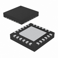
ATA8742-PXQW Atmel, ATA8742-PXQW Datasheet - Page 9

ATA8742-PXQW
Manufacturer Part Number
ATA8742-PXQW
Description
MCU W/TRANSMITTER ASK/FSK 24QFN
Manufacturer
Atmel
Datasheet
1.ATA8742-PXQW.pdf
(238 pages)
Specifications of ATA8742-PXQW
Frequency
433MHz
Applications
Home Automation, Remote Sensing, RKE
Modulation Or Protocol
ASK, FSK
Data Rate - Maximum
32 kBit/s
Power - Output
7.5dBm
Current - Transmitting
9.8mA
Data Interface
PCB, Surface Mount
Antenna Connector
PCB, Surface Mount
Memory Size
4kB Flash, 256B EEPROM, 256B SRAM
Voltage - Supply
2 V ~ 4 V
Operating Temperature
-40°C ~ 85°C
Package / Case
24-VQFN Exposed Pad, 24-HVQFN, 24-SQFN, 24-DHVQFN
Processor Series
ATA8x
Core
AVR8
Data Bus Width
8 bit
Program Memory Type
Flash
Program Memory Size
4 KB
Data Ram Size
256 B
Interface Type
SPI, USI
Maximum Clock Frequency
8.1 MHz
Number Of Programmable I/os
12
Number Of Timers
2
Maximum Operating Temperature
+ 85 C
Mounting Style
SMD/SMT
Development Tools By Supplier
ATASTK512-EK1-IND
Minimum Operating Temperature
- 40 C
On-chip Adc
10 bit, 8 Channel
Lead Free Status / RoHS Status
Lead free / RoHS Compliant
Features
-
Lead Free Status / Rohs Status
Details
Available stocks
Company
Part Number
Manufacturer
Quantity
Price
Company:
Part Number:
ATA8742-PXQW
Manufacturer:
ATMEL
Quantity:
1 482
- Current page: 9 of 238
- Download datasheet (4Mb)
3.4
3.4.1
3.4.2
4. Microcontroller Block
9151A–INDCO–07/09
CLK Output
Clock Pulse Take-over
Output Matching and Power Setting
Using C
tances on each side of the crystal of C
crystal of C
tion of ±21 kHz typical with worst case tolerances of ±16.3 kHz to ±28.8 kHz.
An output CLK signal is provided for the integrated AVR. The delivered signal is CMOS compat-
ible if the load capacitance is lower than 10 pF.
The clock of the crystal oscillator can be used for clocking the microcontroller. Atmel
microcontroller starts with an integrated RC-oscillator to switch on the RF TX with ENABLE = H,
and after 1 ms assumes the clock signal of the transmission IC, so that the message can be sent
with crystal accuracy.
The output power is set by the load impedance of the antenna. The maximum output power is
achieved with a load impedance of Z
to V
The delivered current pulse of the power amplifier is 9 mA and the maximum output power is
delivered to a resistive load of 465 if the 1.0 pF output capacitance of the power amplifier is
compensated by the load impedance.
An optimum load impedance of:
Z
7.5 dBm.
The load impedance is defined as the impedance seen from the RF TX’s ANT1, ANT2 into the
matching network. This large signal load impedance should not be confused with the small sig-
nal input impedance delivered as input characteristic of RF amplifiers and measured from the
application into the IC instead of from the IC into the application for a power amplifier.
Less output power is achieved by lowering the real parallel part of 465 where the parallel imag-
inary part should be kept constant.
Output power measurement can be done using the circuit shown in
that the component values must be changed to compensate the individual board parasitics until
the RF TX has the right load impedance Z
cable used to measure the output power must be calibrated out.
More detailed information about the microcontroller block can be found in the appendix.
Load
S
= 465 || j/(2
to deliver the DC current.
4
= 9.2 pF ±2%, C
0
= 3.2 pF ±10% and a crystal with C
1.0 pF) = (166 + j223) is achieved for the maximum output power of
5
= 6.8 pF ±5%, a switch port with C
Load,opt
Stray1
Load,opt
= (166 + j223) . There must be a low resistive path
= C
Stray2
= (166 + j223) . In addition, the damping of the
M
= 13 fF ±10%, results in a typical FSK devia-
= 1 pF ±10%, a parallel capacitance of the
Switch
Figure 8-4 on page
= 3 pF ±10%, stray capaci-
ATA8742
16. Note
®
’s AVR
9
Related parts for ATA8742-PXQW
Image
Part Number
Description
Manufacturer
Datasheet
Request
R

Part Number:
Description:
Manufacturer:
ATMEL Corporation
Datasheet:

Part Number:
Description:
DEV KIT FOR AVR/AVR32
Manufacturer:
Atmel
Datasheet:

Part Number:
Description:
INTERVAL AND WIPE/WASH WIPER CONTROL IC WITH DELAY
Manufacturer:
ATMEL Corporation
Datasheet:

Part Number:
Description:
Low-Voltage Voice-Switched IC for Hands-Free Operation
Manufacturer:
ATMEL Corporation
Datasheet:

Part Number:
Description:
MONOLITHIC INTEGRATED FEATUREPHONE CIRCUIT
Manufacturer:
ATMEL Corporation
Datasheet:

Part Number:
Description:
AM-FM Receiver IC U4255BM-M
Manufacturer:
ATMEL Corporation
Datasheet:

Part Number:
Description:
Monolithic Integrated Feature Phone Circuit
Manufacturer:
ATMEL Corporation
Datasheet:

Part Number:
Description:
Multistandard Video-IF and Quasi Parallel Sound Processing
Manufacturer:
ATMEL Corporation
Datasheet:

Part Number:
Description:
High-performance EE PLD
Manufacturer:
ATMEL Corporation
Datasheet:

Part Number:
Description:
8-bit Flash Microcontroller
Manufacturer:
ATMEL Corporation
Datasheet:

Part Number:
Description:
2-Wire Serial EEPROM
Manufacturer:
ATMEL Corporation
Datasheet:


