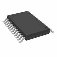
ADF7010BRU Analog Devices Inc, ADF7010BRU Datasheet - Page 6

ADF7010BRU
Manufacturer Part Number
ADF7010BRU
Description
IC TX ASK/FSK/GFSK HP 24-TSSOP
Manufacturer
Analog Devices Inc
Datasheet
1.ADF7010BRUZ-REEL7.pdf
(20 pages)
Specifications of ADF7010BRU
Rohs Status
RoHS non-compliant
Frequency
902MHz ~ 928MHz
Applications
Data Transfer, RKE, Remote Control/Security Systems
Modulation Or Protocol
ASK, FSK, GFSK
Data Rate - Maximum
76.8 kbps
Power - Output
-16dBm ~ 12dBm
Current - Transmitting
40mA
Data Interface
PCB, Surface Mount
Antenna Connector
PCB, Surface Mount
Voltage - Supply
2.3 V ~ 3.6 V
Operating Temperature
-40°C ~ 85°C
Package / Case
24-TSSOP
Operating Temperature (min)
-40C
Operating Temperature (max)
85C
Operating Temperature Classification
Industrial
Product Depth (mm)
4.4mm
Operating Supply Voltage (min)
2.3V
Operating Supply Voltage (typ)
3.3V
Operating Supply Voltage (max)
3.6V
Features
-
Memory Size
-
Lead Free Status / Rohs Status
Not Compliant
Available stocks
Company
Part Number
Manufacturer
Quantity
Price
Part Number:
ADF7010BRUZ
Manufacturer:
ADI/亚德诺
Quantity:
20 000
ADF7010
Pin No.
15
16
17
18
19
20
21
22
23
24
Mnemonic
OSC1
VCO
TEST
DV
RF
RF
A
VCO
C
C
GND
VCO
REG
GND
OUT
DD
GND
IN
Function
Oscillator Pin. For use with crystal reference only. This is three-stated when an external reference oscillator
is used.
Voltage Controlled Oscillator Ground
Input to the RF fractional-N divider. This pin allows the user to connect an external VCO to the part.
Disabling the internal VCO activates this pin. If the internal VCO is used, this pin should be grounded.
Positive Supply for the Digital Circuitry. This must be between 2.3 V and 3.6 V. Decoupling capacitors
to the analog ground plane should be placed as close as possible to this pin.
Ground for Output Stage of Transmitter
The modulated signal is available at this pin. Output power levels are from –16 dBm to +12 dBm. The
output should be impedance matched to the desired load using suitable components. See the Output RF
Stage section.
Ground Pin for the RF Analog Circuitry
The tuning voltage on this pin determines the output frequency of the Voltage Controlled Oscillator
(VCO). The higher the tuning voltage the higher the output frequency.
A 0.22 mF capacitor should be added to reduce noise on VCO bias lines. Tied to C
A 2.2 mF capacitor should be added at C
capacitor will improve regulator power-on time but may cause higher spurious components.
PIN FUNCTION DESCRIPTIONS (continued)
–6–
REG
to reduce regulator noise and improve stability. A reduced
REG
pin.
REV. 0


