IXFN55N50 IXYS, IXFN55N50 Datasheet
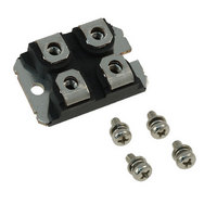
MOSFET N-CH 500V 55A SOT-227B

IXFN55N50

Manufacturer Part Number
IXFN55N50
Description
MOSFET N-CH 500V 55A SOT-227B
Manufacturer
IXYS
Series
HiPerFET™r
Datasheet

Specifications of IXFN55N50

Fet Type
MOSFET N-Channel, Metal Oxide
Fet Feature
Standard
Rds On (max) @ Id, Vgs
90 mOhm @ 500mA, 10V
Drain To Source Voltage (vdss)
500V
Current - Continuous Drain (id) @ 25° C
55A
Vgs(th) (max) @ Id
4.5V @ 8mA
Gate Charge (qg) @ Vgs
330nC @ 10V
Input Capacitance (ciss) @ Vds
9400pF @ 25V
Power - Max
625W
Mounting Type
Chassis Mount
Package / Case
SOT-227, miniBLOC
Configuration
Single
Transistor Polarity
N-Channel
Resistance Drain-source Rds (on)
0.09 Ohms
Drain-source Breakdown Voltage
500 V
Gate-source Breakdown Voltage
+/- 20 V
Continuous Drain Current
55 A
Power Dissipation
625 W
Maximum Operating Temperature
+ 150 C
Mounting Style
SMD/SMT
Minimum Operating Temperature
- 55 C
Vdss, Max, (v)
500
Id(cont), Tc=25°c, (a)
55
Rds(on), Max, Tj=25°c, (?)
0.08
Ciss, Typ, (pf)
9400
Qg, Typ, (nc)
330
Trr, Typ, (ns)
-
Trr, Max, (ns)
250
Pd, (w)
595
Rthjc, Max, (ºc/w)
0.21
Package Style
SOT-227B
Lead Free Status / RoHS Status
Lead free / RoHS Compliant

Available stocks

Company
Part Number
Manufacturer
Quantity
Price
Part Number:
IXFN55N50
Manufacturer:
IXYS
Quantity:
27
Part Number:
IXFN55N50
Manufacturer:
APT
Quantity:
300
© 2004 IXYS All rights reserved
HiPerFET
Power MOSFET
Single Die MOSFET
Symbol
(T
V
V
I
I
R
Symbol
V
V
V
V
I
I
I
E
dv/dt
P
T
T
T
T
M
V
Weight
GSS
DSS
D25
DM
AR
L
DSS
GS(th)
J
JM
stg
DS(on)
DSS
DGR
GSS
GSM
AR
D
ISOL
d
J
= 25°C, unless otherwise specified)
Test Conditions
V
V
V
V
V
Pulse test, t ≤ 300 µs, duty cycle d ≤ 2 %
Test Conditions
T
T
Continuous
Transient
T
T
T
T
I
T
T
1.6 mm (0.062 in.) from case for 10 s (IXFK, IXFX)
Mounting torque
Terminal leads
50/60 Hz, RMS
I
PLUS247
TO-264
SOT-227B
V
S
ISOL
GS
GS
GS
C
C
C
C
C
DS
DS
J
J
J
GS
= 25°C to 150°C
= 25°C to 150°C
= 25°C
= 25°C, pulse width limited by T
= 25°C
= 25°C
≤ I
≤ 150°C, R
= 25°C
≤ ≤ ≤ ≤ ≤
= 0 V, I
= V
= ±20 V
= V
= 0 V
= 10 V, I
DM
1 mA
GS
, di/dt ≤ 100 A/µs, V
DSS
TM
, I
D
D
DC
D
= 1 mA
= 8 mA
, V
= 0.5 I
G
= 4 Ω
DS
= 0
D25
(IXFK, IXFX)
(IXFN)
(IXFN)
DD
T
≤ V
J
= 125°C
DSS
JM
IXFK 55N50
IXFN 55N50
IXFX 55N50
t = 1minute
t = 1 s
500
Min. Typ.
2.5
Characteristic Values
-55 ... +150
-55 ... +150
Maximum Ratings
1.13/10 Nm/lb.in.
1.13/10 Nm/lb.in.
2500
3000
500
500
±20
±30
220
625
150
300
55
55
60
10
10
30
5
±200
Max.
4.5
25
90
2
V/ns
mΩ
mA
nA
µA
mJ
V~
V~
°C
°C
°C
°C
W
V
V
V
V
V
V
A
A
A
g
g
g
TO-264 AA (IXFK)
miniBLOC, SOT-227 B (IXFN)
PLUS247(IXFX)
G = Gate
S = Source
Either Source terminal at miniBLOC can be used
as Main or Kelvin Source
Features
Advantages
International standard packages
Encapsulating epoxy meets
UL 94 V-0, flammability classification
miniBLOC with Aluminium nitride
isolation
Low R
Rugged polysilicon gate cell structure
Unclamped Inductive Switching (UIS)
rated
Low package inductance
Fast intrinsic Rectifier
PLUS247 package for clip or spring
bar mounting
Easy to mount
Space savings
High power density
V
I
R
t
E153432
D25
rr
DSS
DS(on)
DS (on)
G
C
G
E
HDMOS
D
= 500 V
=
S
TAB = Drain
=
D
≤ ≤ ≤ ≤ ≤ 250 ns
G
TM
= Drain
DS97502G(11/04)
process
55 A
90mΩ Ω Ω Ω Ω
S
(TAB)
D
D (TAB)
S

Related parts for IXFN55N50

IXFN55N50 Summary of contents

Page 1

... GSS DSS DS DSS 0.5 I DS(on D25 Pulse test, t ≤ 300 µs, duty cycle d ≤ © 2004 IXYS All rights reserved IXFK 55N50 IXFX 55N50 IXFN 55N50 Maximum Ratings 500 500 ±20 ±30 55 220 ≤ DSS 625 -55 ... +150 150 -55 ... +150 300 1 ...

Page 2

... Max. 55 220 Note 1 1.5 250 = 100 V 1 Terminals Gate 2 - Collector 4,931,844 5,049,961 5,237,481 6,162,665 5,017,508 5,063,307 5,381,025 6,259,123 B1 5,034,796 5,187,117 5,486,715 6,306,728 B1 IXFK55N50 IXFX55N50 IXFN55N50 TO-264 AA Outline Dim. Millimeter Inches Min. Max. Min 4.82 5.13 .190 A1 2.54 2.89 .100 nC A2 2.00 2 ...

Page 3

... Degrees C - Degrees © 2004 IXYS All rights reserved 10V 100 100 120 120 IXF_55N50 75 75 100 125 150 100 125 150 IXFK55N50 IXFX55N50 IXFN55N50 Figure 2. Output Characteristics at 125 100 V = 10V T = 125 Volts DS Figure 4. R normalized to 0.5 DS(on) I value vs. T D25 J 2.2 V ...

Page 4

... Figure 9. Forward Voltage Drop of the Intrinsic Diode 100 125 0.2 0.4 0 Volts SD Figure 10. Transient Thermal Resistance 1.00 0.10 0.01 0. IXFK55N50 Figure 8. Capacitance Curves 10000 1000 100 300 350 0.8 1 Pulse Width - Seconds IXFX55N50 IXFN55N50 Ciss f = 1MHz Coss Crss Volts DS IXFK55N50/IXFX55N50 IXFN55N50 ...

Related keywords