FSB50250US Fairchild Semiconductor, FSB50250US Datasheet
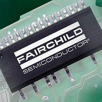
MODULE SPM 500V 1.1A SPM23-BD

FSB50250US

Manufacturer Part Number
FSB50250US
Description
MODULE SPM 500V 1.1A SPM23-BD
Manufacturer
Fairchild Semiconductor
Series
SPM®r
Type
FETr
Datasheet

Specifications of FSB50250US

Configuration
3 Phase
Current
1.1A
Voltage
500V
Voltage - Isolation
1500Vrms
Package / Case
SPM23BD
Mounting Style
SMD/SMT
Maximum Operating Temperature
+ 150 C
Minimum Operating Temperature
- 40 C
Lead Free Status / RoHS Status
Lead free / RoHS Compliant
Other names
FSB50250USTR

Available stocks

Company
Part Number
Manufacturer
Quantity
Price
Part Number:
FSB50250US
Manufacturer:
FSC
Quantity:
1 000
©2009 Fairchild Semiconductor Corporation
FSB50250US Rev. A
FSB50250US
Smart Power Module (SPM
Features
• 500V R
• 3 divided negative dc-link terminals for inverter current sens-
• HVIC for gate driving and undervoltage protection
• 3/5V CMOS/TTL compatible, active-high interface
• Optimized for low electromagnetic interference
• Isolation voltage rating of 1500Vrms for 1min.
• Surface mounted device package
• Moisture Sensitive Level (MSL) 3
Absolute Maximum Ratings
Symbol
high voltage integrated circuit (HVIC)
ing applications
T
R
V
V
V
I
I
V
I
V
P
D25
D80
T
STG
DP
θJC
ISO
CC
PN
BS
IN
D
J
DS(on)
DC Link Input Voltage,
Drain-source Voltage of each FRFET
Each FRFET Drain Current, Continuous
Each FRFET Drain Current, Peak
Maximum Power Dissipation
Control Supply Voltage
High-side Bias Voltage
Input Signal Voltage
Operating Junction Temperature
Storage Temperature
Junction to Case Thermal Resistance
Isolation Voltage
=4.2Ω(max) 3-phase FRFET inverter including
Parameter
®
)
T
T
T
T
Applied between V
Applied between V
Applied between IN and COM
Each FRFET under inverter operating con-
dition (Note 1)
60Hz, Sinusoidal, 1 minute, Connection
pins to heatsink
C
C
C
C
= 25°C
= 80°C
= 25°C, PW < 100μs
= 25°C, Each FRFET
1
General Description
FSB50250US is a tiny smart power module (SPM
FRFET technology as a compact inverter solution for small
power motor drive applications such as fan motors and water
suppliers. It is composed of 6 fast-recovery MOSFET (FRFET),
and 3 half-bridge HVICs for FRFET gate driving. FSB50250US
provides low electromagnetic interference (EMI) characteristics
with optimized switching speed. Moreover, since it employs
FRFET as a power switch, it has much better ruggedness and
larger safe operation area (SOA) than that of an IGBT-based
power module or one-chip solution. The package is optimized
for the thermal performance and compactness for the use in the
built-in motor application and any other application where the
assembly space is concerned. FSB50250US is the most
solution for the compact inverter providing the energy efficiency,
compactness, and low electromagnetic interference.
Conditions
CC
B(U)
and COM
-U, V
B(V)
-V, V
B(W)
-W
-0.3 ~ VCC+0.3
-40 ~ 150
-50 ~ 150
Rating
1500
500
1.1
0.8
2.8
9.3
13
20
20
February 2009
www.fairchildsemi.com
®
) based on
Units
°C/W
V
°C
°C
W
V
A
A
A
V
V
V
rms

Related parts for FSB50250US

FSB50250US Summary of contents

Page 1

... FRFET technology as a compact inverter solution for small power motor drive applications such as fan motors and water suppliers composed of 6 fast-recovery MOSFET (FRFET), and 3 half-bridge HVICs for FRFET gate driving. FSB50250US provides low electromagnetic interference (EMI) characteristics with optimized switching speed. Moreover, since it employs ...

Page 2

... Note: Source terminal of each low-side MOSFET is not connected to supply ground or bias voltage ground inside SPM ure 2 and 5. Figure 1. Pin Configuration and Internal Block Diagram (Bottom View) FSB50250US Rev. A Pin Description IC Common Supply Ground Bias Voltage for U Phase High Side FRFET Driving ...

Page 3

... The peak current and voltage of each FRFET during the switching operation should be included in the safe operating area (SOA). Please see Figure 5 for the RBSOA test cir- cuit that is same as the switching test circuit. Package Marking & Ordering Information Device Marking Device FSB50250US FSB50250US FSB50250US Rev 25° =15V Unless Otherwise Specified ...

Page 4

... Figure 2. Recommended CPU Interface and Bootstrap Circuit with Parameters 3.80mm 3.80mm Note: Attach the thermocouple on top of the heatsink-side of SPM FSB50250US Rev. A Conditions Applied between P and N Applied between V and COM CC Applied between V and output( ...

Page 5

... V IN 100 (a) Turn- Figure 5. Switching and RBSOA(Single-pulse) Test Circuit (Low-side) Input Signal UV Protection Status Low-side Supply, V MOSFET Current Input Signal UV Protection Status High-side Supply, V MOSFET Current FSB50250US Rev 120 Figure 4. Switching Time Definition R EH VCC VB HIN HO LIN VS COM LO C One-leg Diagram of SPM ...

Page 6

... 15-V Supply FSB50250US Rev (1) COM (2) V B(U) (3) V CC(U) VCC VB (4) IN (UH) HIN HO (5) IN (UL) LIN VS C COM LO 1 (6) V S(U) (7) V B(V) (8) V CC(V) VCC VB (9) IN (VH) HIN HO (10) IN (VL) LIN VS C COM LO 1 (11) V S(V) (12) V B(W) (13) V CC(W) ...

Page 7

... Detailed Package Outline Drawings (1.165) 15*1.778=26.67 13.34 ±0.30 #1 #17 12.23 ±0.30 2x3.90=7.80 (2.275) 0.60 ±0.10 Max 1.00 GAGE PLANE SEATING PLANE FSB50250US Rev. A Max 1.00 0.60 ±0.10 ±0.30 13.34 ±0.30 #1 #16 1.30 #23 13.13 ±0.30 7.80 29.00 ±0.20 LAND PATTERN RECOMMENDATIONS ±0.30 4x3.90=15.60 ± ...

Page 8

... Datasheet Identification Product Status Advance Information Formative or In Design Preliminary First Production No Identification Needed Full Production Obsolete Not In Production FSB50250US Rev. A GlobalOptoisolator™ Power247 GTO™ PowerEdge™ HiSeC™ PowerSaver™ i-Lo™ PowerTrench ImpliedDisconnect™ Programmable Active Droop™ ...

Related keywords