MPXH6400A6T1 Freescale Semiconductor, MPXH6400A6T1 Datasheet - Page 6
MPXH6400A6T1
Manufacturer Part Number
MPXH6400A6T1
Description
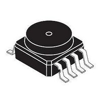
SENSOR PRESSURE ABSOLUTE 8-SSOP
Manufacturer
Freescale Semiconductor
Series
MPXH6400r
Specifications of MPXH6400A6T1
Pressure Type
Absolute
Operating Pressure
3 ~ 58 PSI
Output
0 ~ 4.8V
Voltage - Supply
4.85 V ~ 5.35 V
Termination Style
PCB
Operating Temperature
-40°C ~ 125°C
Package / Case
8-SSOP without Port
Mounting Style
SMD/SMT
Maximum Operating Temperature
+ 125 C
Minimum Operating Temperature
- 40 C
Operating Supply Voltage
5 V
Output Voltage
4.733 V to 4.866 V
Lead Free Status / RoHS Status
Lead free / RoHS Compliant


MPXH6400A
6
the Pressure (P1) side and the Vacuum (P2) side. The
Pressure (P1) side is the side containing fluorosilicone gel,
which protects the die from harsh media. The MPX pressure
design. The footprint for the surface mount packages must be
the correct size to ensure proper solder connection interface
between the board and the package. With the correct
design. The footprint for the semiconductor package must be
the correct size to ensure proper solder connection interface
between the board and the package. With the correct pad
geometry, the packages will self-align when subjected to a
solder reflow process. It is always recommended to fabricate
boards with a solder mask layer to avoid bridging and/or
shorting between solder pads, especially on tight tolerances
and/or tight layouts.
Surface mount board layout is a critical portion of the total
Surface mount board layout is a critical portion of the total
The two sides of the pressure sensor are designated as
Pressure
MPXH6400AC6U
MPXH6400AC6T1
MPXHZ6400AC6T1
MPXA6400AP
PRESSURE (P1)/VACUUM (P2) SIDE IDENTIFICATION TABLE
0.060 TYP 8X
1.52
Minimum Recommended Footprint for Super Small Outline Package
Minimum Recommended Footprint for Small Outline Package
Part Number
SURFACE MOUNTING INFORMATION
Figure 4. SOP Footprint (Case 1369)
0.100 TYP 8X
2.54
0.660
16.76
Case Type
1317A
1317A
1317A
1369
sensor is designed to operate with positive differential
pressure applied, P1 > P2.
following table:
footprint, the packages will self align when subjected to a
solder reflow process. It is always recommended to design
boards with a solder mask layer to avoid bridging and
shorting between solder pads.
The Pressure (P1) side may be identified by using the
0.150
3.81
Side with Port Attached
Side with Port Attached
Side with Port Attached
Side with Port Attached
Figure 5. SSOP Footprint (Case 1317A)
Pressure (P1) Side Identifier
inch
mm
SCALE 2:1
0.100 TYP 8X
2.54
0.050
0.300
1.27
TYP
7.62
0.053 TYP 8X
1.35
Freescale Semiconductor
0.387
0.027 TYP 8X
9.83
0.69
inch
mm
Sensors
Related parts for MPXH6400A6T1
Image
Part Number
Description
Manufacturer
Datasheet
Request
R

Part Number:
Description:
SENSOR ABS PRESS 58PSI MAX
Manufacturer:
Freescale Semiconductor
Datasheet:

Part Number:
Description:
PRESSURE SENSOR ABS AXIAL 8-SSOP
Manufacturer:
Freescale Semiconductor
Datasheet:

Part Number:
Description:
SENSOR PRESSURE ABSOLUTE 8-SSOP
Manufacturer:
Freescale Semiconductor
Datasheet:

Part Number:
Description:
Manufacturer:
Freescale Semiconductor, Inc
Datasheet:
Part Number:
Description:
Manufacturer:
Freescale Semiconductor, Inc
Datasheet:
Part Number:
Description:
Manufacturer:
Freescale Semiconductor, Inc
Datasheet:
Part Number:
Description:
Manufacturer:
Freescale Semiconductor, Inc
Datasheet:
Part Number:
Description:
Manufacturer:
Freescale Semiconductor, Inc
Datasheet:
Part Number:
Description:
Manufacturer:
Freescale Semiconductor, Inc
Datasheet:
Part Number:
Description:
Manufacturer:
Freescale Semiconductor, Inc
Datasheet:
Part Number:
Description:
Manufacturer:
Freescale Semiconductor, Inc
Datasheet:
Part Number:
Description:
Manufacturer:
Freescale Semiconductor, Inc
Datasheet:
Part Number:
Description:
Manufacturer:
Freescale Semiconductor, Inc
Datasheet:
Part Number:
Description:
Manufacturer:
Freescale Semiconductor, Inc
Datasheet:
Part Number:
Description:
Manufacturer:
Freescale Semiconductor, Inc
Datasheet: