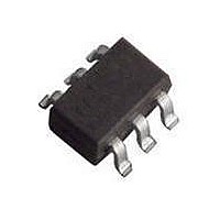
BF1205,115 NXP Semiconductors, BF1205,115 Datasheet - Page 11

BF1205,115
Manufacturer Part Number
BF1205,115
Description
MOSFET 2N-CH 10V 30MA SOT363
Manufacturer
NXP Semiconductors
Datasheet
1.BF1205135.pdf
(25 pages)
Specifications of BF1205,115
Package / Case
6-TSSOP, SC-88, SOT-363
Current Rating
30mA
Frequency
800MHz
Gain
35dB
Transistor Type
N-Channel Dual Gate
Noise Figure
1.2dB
Current - Test
12mA
Voltage - Test
5V
Configuration
Dual
Transistor Polarity
Dual N-Channel
Drain-source Breakdown Voltage
10 V
Continuous Drain Current
30 mA
Power Dissipation
200 mW
Mounting Style
SMD/SMT
Lead Free Status / RoHS Status
Lead free / RoHS Compliant
Power - Output
-
Lead Free Status / RoHS Status
Lead free / RoHS Compliant, Lead free / RoHS Compliant
NXP Semiconductors
2003 Sep 30
handbook, halfpage
handbook, halfpage
Dual N-channel dual gate MOS-FET
V
I
Fig.14 Input admittance as a function of frequency;
V
I
Fig.16 Reverse transfer admittance and phase as
D
D
DS
DS
(mS)
(a) = 12 mA.
(a) = 12 mA.
|
10 −
10 −
(μS)
y is
y rs
10
10
10
(a) = 5 V; V
(a) = 5 V; V
10
10
1
|
1
2
1
2
3
2
10
10
typical values; amplifier a.
a function of frequency; typical values;
amplifier a.
G2-S
G2-S
(a) = 4 V; V
(a) = 4 V; V
DS
DS
10
10
(b) = V
(b) = V
2
2
ϕ rs
|
b is
g is
y rs
|
G1-S
G1-S
f (MHz)
f (MHz)
(b) = 0 V;
(b) = 0 V;
MGX441
MGX443
10
10
3
3
−10
−10
−10
−1
(deg)
ϕ rs
3
2
11
handbook, halfpage
handbook, halfpage
V
I
Fig.15 Forward transfer admittance and phase as
V
I
Fig.17 Output admittance as a function of
D
D
DS
DS
(mS)
(a) = 12 mA.
(a) = 12 mA.
(mS)
|
y os
10 −
10 −
y fs
10
(a) = 5 V; V
(a) = 5 V; V
10
10
1
|
1
2
1
2
10
10
a function of frequency; typical values;
amplifier a.
frequency; typical values; amplifier a.
G2-S
G2-S
(a) = 4 V; V
(a) = 4 V; V
DS
DS
10
10
2
(b) = V
2
(b) = V
|
y fs
b os
g os
ϕ fs
|
G1-S
G1-S
f (MHz)
f (MHz)
Product specification
(b) = 0 V;
(b) = 0 V;
BF1205
MGX442
MGX444
10
10
3
3
−10
−10
−1
(deg)
ϕ fs
2


