NUC100LC1BN Nuvoton Technology Corporation of America, NUC100LC1BN Datasheet - Page 3
NUC100LC1BN
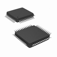
Manufacturer Part Number
NUC100LC1BN
Description
IC MCU 32BIT 32KB FLASH 48LQFP
Manufacturer
Nuvoton Technology Corporation of America
Series
NuMicro™r
Specifications of NUC100LC1BN
Core Processor
ARM Cortex-M0
Core Size
32-Bit
Speed
50MHz
Connectivity
I²C, IrDA, SPI, UART/USART
Peripherals
Brown-out Detect/Reset, DMA, I²S, LVD, POR, PS2, PWM, WDT
Number Of I /o
35
Program Memory Size
32KB (32K x 8)
Program Memory Type
FLASH
Ram Size
4K x 8
Voltage - Supply (vcc/vdd)
2.5 V ~ 5.5 V
Data Converters
A/D 8x12b
Oscillator Type
Internal
Operating Temperature
-40°C ~ 85°C
Package / Case
48-LQFP
Lead Free Status / RoHS Status
Lead free / RoHS Compliant
Eeprom Size
-
Available stocks
Company
Part Number
Manufacturer
Quantity
Price
Company:

Part Number:
NUC100LC1BN
Manufacturer:
NuvoTon
Quantity:
1 600
Company:
Part Number:
NUC100LC1BN
Manufacturer:
Nuvoton Technology Corporation of America
Quantity:
10 000
Part Number:
NUC100LC1BN
Manufacturer:
NUVOTON
Quantity:
20 000


5.3
5.4
5.5
5.6
5.7
5.8
5.2.2
5.2.3
5.2.4
5.2.5
5.2.6
5.2.7
5.2.8
Clock Controller .......................................................................................................... 191
5.3.1
5.3.2
5.3.3
5.3.4
5.3.5
5.3.6
5.3.7
5.3.8
USB Device Controller (USB) ..................................................................................... 215
5.4.1
5.4.2
5.4.3
5.4.4
5.4.5
5.4.6
General Purpose I/O................................................................................................... 240
5.5.1
5.5.2
5.5.3
5.5.4
5.5.5
I
5.6.1
5.6.2
5.6.3
5.6.4
5.6.5
5.6.6
5.6.7
5.6.8
PWM Generator and Capture Timer (PWM) .............................................................. 283
5.7.1
5.7.2
5.7.3
5.7.4
5.7.5
5.7.6
Real Time Clock (RTC)............................................................................................... 322
5.8.1
NuMicro™ NUC100 Series Technical Reference Manual
2
C Serial Interface Controller (Master/Slave) (I
System Reset ...............................................................................................................113
System Power Distribution ...........................................................................................114
System Memory Map....................................................................................................116
System Manager Control Registers..............................................................................118
System Timer (SysTick) ...............................................................................................154
Nested Vectored Interrupt Controller (NVIC) ................................................................159
System Control Register...............................................................................................183
Overview ......................................................................................................................191
Clock Generator ...........................................................................................................191
System Clock & SysTick Clock.....................................................................................192
Peripherals Clock .........................................................................................................193
Power down mode (Deep Sleep Mode) Clock..............................................................193
Frequency Divider Output.............................................................................................194
Register Map ................................................................................................................195
Register Description .....................................................................................................196
Overview ......................................................................................................................215
Features .......................................................................................................................215
Block Diagram ..............................................................................................................216
Function Description.....................................................................................................217
Register and Memory Map ...........................................................................................221
Register Description .....................................................................................................223
Overview ......................................................................................................................240
Features .......................................................................................................................240
Function Description.....................................................................................................241
Register Map ................................................................................................................243
Register Description .....................................................................................................247
Overview ......................................................................................................................259
Features .......................................................................................................................260
Function Description.....................................................................................................261
Protocol Registers ........................................................................................................264
Register Map ................................................................................................................267
Register Description .....................................................................................................268
Modes of Operation ......................................................................................................276
Data Transfer Flow in Five Operating Modes ...............................................................277
Overview ......................................................................................................................283
Features .......................................................................................................................284
Block Diagram ..............................................................................................................285
Function Description.....................................................................................................289
Register Map ................................................................................................................296
Register Description .....................................................................................................299
Overview ......................................................................................................................322
- 3 -
2
C) .................................................... 259
Publication Release Date: Oct 22, 2010
Revision V1.06
Related parts for NUC100LC1BN
Image
Part Number
Description
Manufacturer
Datasheet
Request
R

Part Number:
Description:
Manufacturer:
Nuvoton Technology Corporation of America
Datasheet:
Part Number:
Description:
Manufacturer:
Nuvoton Technology Corporation of America
Datasheet:
Part Number:
Description:
Manufacturer:
Nuvoton Technology Corporation of America
Datasheet:
Part Number:
Description:
Manufacturer:
Nuvoton Technology Corporation of America
Datasheet:
Part Number:
Description:
Manufacturer:
Nuvoton Technology Corporation of America
Datasheet:
Part Number:
Description:
Manufacturer:
Nuvoton Technology Corporation of America
Datasheet:
Part Number:
Description:
Manufacturer:
Nuvoton Technology Corporation of America
Datasheet: