NUC100LC1BN Nuvoton Technology Corporation of America, NUC100LC1BN Datasheet - Page 8
NUC100LC1BN
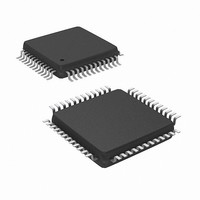
Manufacturer Part Number
NUC100LC1BN
Description
IC MCU 32BIT 32KB FLASH 48LQFP
Manufacturer
Nuvoton Technology Corporation of America
Series
NuMicro™r
Specifications of NUC100LC1BN
Core Processor
ARM Cortex-M0
Core Size
32-Bit
Speed
50MHz
Connectivity
I²C, IrDA, SPI, UART/USART
Peripherals
Brown-out Detect/Reset, DMA, I²S, LVD, POR, PS2, PWM, WDT
Number Of I /o
35
Program Memory Size
32KB (32K x 8)
Program Memory Type
FLASH
Ram Size
4K x 8
Voltage - Supply (vcc/vdd)
2.5 V ~ 5.5 V
Data Converters
A/D 8x12b
Oscillator Type
Internal
Operating Temperature
-40°C ~ 85°C
Package / Case
48-LQFP
Lead Free Status / RoHS Status
Lead free / RoHS Compliant
Eeprom Size
-
Available stocks
Company
Part Number
Manufacturer
Quantity
Price
Company:

Part Number:
NUC100LC1BN
Manufacturer:
NuvoTon
Quantity:
1 600
Company:
Part Number:
NUC100LC1BN
Manufacturer:
Nuvoton Technology Corporation of America
Quantity:
10 000
Part Number:
NUC100LC1BN
Manufacturer:
NUVOTON
Quantity:
20 000


Figure 5-6 SysTick Clock Control Block Diagram ........................................................................ 192
Figure 5-7 Clock Source of Frequency Divider ............................................................................ 194
Figure 5-8 Block Diagram of Frequency Divider .......................................................................... 194
Figure 5-9 USB Block Diagram .................................................................................................... 216
Figure 5-10 Wakeup Interrupt Operation Flow............................................................................ 218
Figure 5-11 Endpoint SRAM Structure ........................................................................................ 219
Figure 5-12 Setup Transaction followed by Data in Transaction ................................................. 220
Figure 5-13 Data Out Transfer ..................................................................................................... 220
Figure 5-14 Push-Pull Output....................................................................................................... 241
Figure 5-15 Open-Drain Output ................................................................................................... 242
Figure 5-16 Quasi-bidirectional I/O Mode .................................................................................... 242
Figure 5-17 I
Figure 5-18 I
Figure 5-19 Master Transmits Data to Slave ............................................................................... 261
Figure 5-20 Master Reads Data from Slave ................................................................................ 261
Figure 5-21 START and STOP condition..................................................................................... 262
Figure 5-22 Bit Transfer on the I
Figure 5-23 Acknowledge on the I
Figure 5-24 I
Figure 5-25: I
Figure 5-26 Legend for the following five figures ......................................................................... 277
Figure 5-27 Master Transmitter Mode ......................................................................................... 278
Figure 5-28 Master Receiver Mode.............................................................................................. 279
Figure 5-29 Slave Transmitter Mode............................................................................................ 280
Figure 5-30 Slave Receiver Mode................................................................................................ 281
Figure 5-31 GC Mode .................................................................................................................. 282
Figure 5-32 PWM Generator 0 Clock Source Control.................................................................. 285
Figure 5-33 PWM Generator 0 Architecture Diagram.................................................................. 285
Figure 5-34 PWM Generator 2 Clock Source Control.................................................................. 286
Figure 5-35 PWM Generator 2 Architecture Diagram.................................................................. 286
Figure 5-36 PWM Generator 4 Clock Source Control.................................................................. 287
Figure 5-37 PWM Generator 4 Architecture Diagram.................................................................. 287
Figure 5-38 PWM Generator 6 Clock Source Control.................................................................. 288
Figure 5-39 PWM Generator 6 Architecture Diagram.................................................................. 288
Figure 5-40 Legend of Internal Comparator Output of PWM-Timer ............................................ 289
Figure 5-41 PWM-Timer Operation Timing.................................................................................. 290
Figure 5-42 PWM Double Buffering Illustration............................................................................ 290
NuMicro™ NUC100 Series Technical Reference Manual
2
2
2
2
C Bus Timing .......................................................................................................... 259
C Protocol............................................................................................................... 261
C Data Shifting Direction ........................................................................................ 265
C Time-out Count Block Diagram ......................................................................... 266
2
C bus ....................................................................................... 263
2
C bus..................................................................................... 263
- 8 -
Publication Release Date: Dec. 22, 2010
Revision V1.06
Related parts for NUC100LC1BN
Image
Part Number
Description
Manufacturer
Datasheet
Request
R

Part Number:
Description:
Manufacturer:
Nuvoton Technology Corporation of America
Datasheet:
Part Number:
Description:
Manufacturer:
Nuvoton Technology Corporation of America
Datasheet:
Part Number:
Description:
Manufacturer:
Nuvoton Technology Corporation of America
Datasheet:
Part Number:
Description:
Manufacturer:
Nuvoton Technology Corporation of America
Datasheet:
Part Number:
Description:
Manufacturer:
Nuvoton Technology Corporation of America
Datasheet:
Part Number:
Description:
Manufacturer:
Nuvoton Technology Corporation of America
Datasheet:
Part Number:
Description:
Manufacturer:
Nuvoton Technology Corporation of America
Datasheet: