S9S08LG32J0VLF Freescale Semiconductor, S9S08LG32J0VLF Datasheet - Page 24
S9S08LG32J0VLF
Manufacturer Part Number
S9S08LG32J0VLF
Description
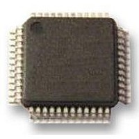
IC MCU 8BIT 32KB FLASH 48LQFP
Manufacturer
Freescale Semiconductor
Series
HCS08r
Datasheet
1.DEMO9S08LG32.pdf
(50 pages)
Specifications of S9S08LG32J0VLF
Core Processor
HCS08
Core Size
8-Bit
Speed
40MHz
Connectivity
I²C, LIN, SCI, SPI
Peripherals
LCD, LVD, POR, PWM, WDT
Number Of I /o
39
Program Memory Size
32KB (32K x 8)
Program Memory Type
FLASH
Ram Size
1.9K x 8
Voltage - Supply (vcc/vdd)
2.7 V ~ 5.5 V
Data Converters
A/D 9x12b
Oscillator Type
Internal
Operating Temperature
-40°C ~ 105°C
Package / Case
48-LQFP
Processor Series
S08LG
Core
HCS08
Data Bus Width
8 bit
Data Ram Size
2 KB
Interface Type
I2C, SCI, SPI
Maximum Clock Frequency
40 MHz
Number Of Programmable I/os
39
Operating Supply Voltage
2.7 V to 5.5 V
Maximum Operating Temperature
+ 105 C
Mounting Style
SMD/SMT
3rd Party Development Tools
EWS08
Development Tools By Supplier
DEMO9S08LG32
Minimum Operating Temperature
- 40 C
On-chip Adc
12 bit, 16 Channel
Lead Free Status / RoHS Status
Lead free / RoHS Compliant
Eeprom Size
-
Lead Free Status / Rohs Status
Details
Available stocks
Company
Part Number
Manufacturer
Quantity
Price
Company:

Part Number:
S9S08LG32J0VLF
Manufacturer:
Freescale Semiconductor
Quantity:
10 000
Part Number:
S9S08LG32J0VLF
Manufacturer:
FREESCALE
Quantity:
20 000


1
2
3
4
5
Electrical Characteristics
2.9
24
Num
10
11
1
2
3
4
5
6
7
8
9
Data in Typical column was characterized at 5.0 V, 25 °C or is typical recommended value.
The resulting bus clock frequency should not exceed the maximum specified bus clock frequency of the device.
This parameter is characterized and not tested on each device.
This specification applies to any time the FLL reference source or reference divider is changed, trim value changed or changing
from FLL disabled (FBELP, FBILP) to FLL enabled (FEI, FEE, FBE, FBI). If a crystal/resonator is being used as the reference,
this specification assumes it is already running.
Jitter is the average deviation from the programmed frequency measured over the specified interval at maximum f
Measurements are made with the device powered by filtered supplies and clocked by a stable external clock signal. Noise
injected into the FLL circuitry via V
for a given interval.
C
C
C
C
C
C
C
C
C
P
P
P
P
P
Table 11. ICS Frequency Specifications (Temperature Range = –40 °C to 105 °C Ambient)
Internal Clock Source (ICS) Characteristics
Average internal reference frequency — factory trimmed
at VDD = 5.0 V and temperature = 25
Average internal reference frequency — user trimmed
Internal reference start-up time
DCO output frequency range —
trimmed
DCO output frequency
Reference = 32768 Hz
and
DMX32 = 1
Resolution of trimmed DCO output frequency at fixed
voltage and temperature (using FTRIM)
Resolution of trimmed DCO output frequency at fixed
voltage and temperature (not using FTRIM)
Total deviation of trimmed DCO output frequency over
voltage and temperature
Total deviation of trimmed DCO output frequency over
fixed voltage and temperature range of 0
FLL acquisition time
Long term jitter of DCO output clock (averaged over 2 ms
interval)
Figure 16. Typical Crystal or Resonator Circuit: Low Range/Low Power
5
2
3, 4
Characteristic
2
DD
3
and V
EXTAL
MC9S08LG32 Series Data Sheet, Rev. 7
SS
Low range (DRS = 00)
Mid range (DRS = 01)
Low range (DRS = 00)
Mid range (DRS = 01)
and variation in the crystal oscillator frequency increase the C
°
C
3
Crystal or Resonator
°
C to 70
3
XOSC
°
C
3
f
Δf
Δf
dco_DMX32
Symbol
t
Δf
Δf
dco_res_t
dco_res_t
Acquire
C
f
t
f
f
dco_t
int_ft
IRST
int_t
dco_t
dco_t
Jitter
XTAL
31.25
Min
16
32
—
—
—
—
—
—
—
—
—
—
32.768
to +0.5
19.92
39.85
Typ
±0.1
±0.2
–1.0
±0.5
0.02
60
—
—
—
—
Freescale Semiconductor
1
39.0625
Jitter
Max
±0.2
±0.4
100
0.2
20
40
±2
±1
—
—
—
1
percentage
Bus
.
%f
%f
%f
%f
%f
Unit
MHz
MHz
kHz
kHz
mS
μs
dco
dco
dco
dco
dco
Related parts for S9S08LG32J0VLF
Image
Part Number
Description
Manufacturer
Datasheet
Request
R

Part Number:
Description:
Manufacturer:
Freescale Semiconductor, Inc
Datasheet:
Part Number:
Description:
Manufacturer:
Freescale Semiconductor, Inc
Datasheet:
Part Number:
Description:
Manufacturer:
Freescale Semiconductor, Inc
Datasheet:
Part Number:
Description:
Manufacturer:
Freescale Semiconductor, Inc
Datasheet:
Part Number:
Description:
Manufacturer:
Freescale Semiconductor, Inc
Datasheet:
Part Number:
Description:
Manufacturer:
Freescale Semiconductor, Inc
Datasheet:
Part Number:
Description:
Manufacturer:
Freescale Semiconductor, Inc
Datasheet:
Part Number:
Description:
Manufacturer:
Freescale Semiconductor, Inc
Datasheet:
Part Number:
Description:
Manufacturer:
Freescale Semiconductor, Inc
Datasheet:
Part Number:
Description:
Manufacturer:
Freescale Semiconductor, Inc
Datasheet:
Part Number:
Description:
Manufacturer:
Freescale Semiconductor, Inc
Datasheet:
Part Number:
Description:
Manufacturer:
Freescale Semiconductor, Inc
Datasheet:
Part Number:
Description:
Manufacturer:
Freescale Semiconductor, Inc
Datasheet:
Part Number:
Description:
Manufacturer:
Freescale Semiconductor, Inc
Datasheet:
Part Number:
Description:
Manufacturer:
Freescale Semiconductor, Inc
Datasheet: