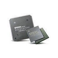
S1D13743F00A200 Epson, S1D13743F00A200 Datasheet - Page 25

S1D13743F00A200
Manufacturer Part Number
S1D13743F00A200
Description
LCD Drivers LCD CNTRL w/Embedded 464KB SRAM
Manufacturer
Epson
Datasheet
1.S1D13743F00A200.pdf
(134 pages)
Specifications of S1D13743F00A200
Maximum Clock Frequency
33 MHz, 68.59 MHz
Operating Supply Voltage
1.5 V
Maximum Operating Temperature
+ 85 C
Package / Case
QFP-20-144
Attached Touch Screen
No
Maximum Supply Current
74 mA
Minimum Operating Temperature
- 40 C
Lead Free Status / RoHS Status
Lead free / RoHS Compliant
Available stocks
Company
Part Number
Manufacturer
Quantity
Price
Company:
Part Number:
S1D13743F00A200
Manufacturer:
EPSON
Quantity:
5 690
- Current page: 25 of 134
- Download datasheet (3Mb)
Epson Research and Development
Vancouver Design Center
1. The minimum System Clock frequency required for correct operation depends on the cycle length of the
2. The input clock period jitter is the displacement relative to the center period (reciprocal of the center
3. The input clock cycle jitter is the difference in period between adjacent cycles.
4. The jitter characteristics must satisfy both the t5 and t6 characteristics.
5. Input Duty cycle is not critical and can be 40/60.
6. t6 = 2 x t
7.1.2 PLL Clock
Hardware Functional Specification
Issue Date: 2010/05/18
(see Note 6)
(see note 1)
Symbol
f
t
Intel 80 interface. See Section 9.4, “Setting SYSCLK and PCLK” on page 43 for more details.
frequency).
OSC
OSC
t1
t2
t3
t4
t5
t6
OSC
Input clock frequency - PLL used for System Clock
Input clock frequency - CLKI used for System Clock
Input clock period
Input clock pulse width high
Input clock pulse width low
Input clock rise time (10% ~ 90%)
Input clock fall time (90% ~ 10%)
Input clock period jitter (see Notes 2 and 4)
Input clock cycle jitter (see Notes 3 and 4)
The PLL circuit is an analog circuit and is very sensitive to noise on the input clock
waveform or the power supply. Noise on the clock or the supplied power may cause the
operation of the PLL circuit to become unstable or increase the jitter.
Due to these noise constraints, it is highly recommended that the power supply traces or the
power plane for the PLL be isolated from those of other power supplies. Filtering should
also be used to keep the power as clean as possible. The jitter of the input clock waveform
should be as small as possible.
Table 7-1 Clock Input Requirements (CLKI)
Parameter
Revision 2.7
0.4t
0.4t
-300
-300
Min
—
—
—
1
0
OSC
OSC
1/f
Typ
—
—
—
—
—
—
OSC
0.6t
0.6t
68.59
Max
300
300
5.0
5.0
33
—
OSC
OSC
X70A-A-001-02
S1D13743
Units
MHz
MHz
Page 25
μs
μs
μs
ns
ns
ps
ps
Related parts for S1D13743F00A200
Image
Part Number
Description
Manufacturer
Datasheet
Request
R

Part Number:
Description:
Display Modules & Development Tools S1D13743 Eval board
Manufacturer:
Epson

Part Number:
Description:
INK CARTRIDGE, T0803, EPSON, MAG
Manufacturer:
Epson
Datasheet:

Part Number:
Description:
INK CARTRIDGE, T0804, EPSON, YEL
Manufacturer:
Epson
Datasheet:

Part Number:
Description:
CXA1034M
Manufacturer:
EPSON Electronics
Datasheet:

Part Number:
Description:
Manufacturer:
EPSON Electronics
Datasheet:

Part Number:
Description:
Manufacturer:
EPSON Electronics
Datasheet:

Part Number:
Description:
Manufacturer:
EPSON Electronics
Datasheet:

Part Number:
Description:
Manufacturer:
EPSON Electronics
Datasheet:

Part Number:
Description:
RTC58321Real time clock module(4-bit I/O CONNECTION REAL TIME CLOCK MODULE)
Manufacturer:
EPSON Electronics
Datasheet:

Part Number:
Description:
SCI7661DC-DC Converter
Manufacturer:
EPSON Electronics
Datasheet:

Part Number:
Description:
Manufacturer:
EPSON Electronics
Datasheet:

Part Number:
Description:
Manufacturer:
EPSON Electronics
Datasheet:


