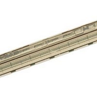
TSL1401CS-LF TAOS, TSL1401CS-LF Datasheet
TSL1401CS-LF
Specifications of TSL1401CS-LF
Available stocks


Related parts for TSL1401CS-LF


TSL1401CS-LF Summary of contents
Page 1
... Available in a Solder-Bump Linear Array Package D Lead (Pb) Free and RoHS Compliant Description The TSL1401CS−LF linear sensor array consists of a 128 × 1 array of photodiodes, associated charge amplifier circuitry, and a pixel data-hold function that provides simultaneous-integration start and stop times for all pixels. The pixels measure 63.5 μ ...
Page 2
... A 0.1 μF bypass capacitor should be connected between V The TSL1401CS−LF is intended for use in a wide variety of applications, including: image scanning, mark and code reading, optical character recognition (OCR) and contact imaging, edge detection and positioning, and optical linear and rotary encoding. ...
Page 3
... TSL1401CS−LF TAOS072E − APRIL 2007 ORDERING NUMBER TSL1401CS−LF −0 −0 0.3V DD − − ...
Page 4
... TSL1401CS−LF 128 × 1 LINEAR SENSOR ARRAY WITH HOLD TAOS072E − APRIL 2007 Electrical Characteristics at f clock 330 Ω μW/cm (unless otherwise noted) (see Note 3 and Note PARAMETER V Analog output voltage (white, average over 128 pixels) See Note 4 out V Analog output voltage (dark, average over 128 pixels) ...
Page 5
... TEST CONDITIONS R = 330 Ω, L TYPICAL CHARACTERISTICS t Integrating 129 Clock Cycles Figure 1. Timing Waveforms 2 128 t pd(SO) Pixel 128 Figure 2. Operational Waveforms r www.taosinc.com TSL1401CS−LF TAOS072E − APRIL 2007 MIN TYP MAX UNIT 120 int Î Î Î Î Î Î Î Î ...
Page 6
... TSL1401CS−LF 128 × 1 LINEAR SENSOR ARRAY WITH HOLD TAOS072E − APRIL 2007 PHOTODIODE SPECTRAL RESPONSIVITY 25°C A 0.8 0.6 0.4 0.2 0 300 400 500 600 700 800 λ − Wavelength − nm Figure 3 AVERAGE ANALOG OUTPUT VOLTAGE, WHITE vs FREE-AIR TEMPERATURE 3.50 t int 3 ...
Page 7
... TYPICAL CHARACTERISTICS 600 out 500 470 pF 400 220 pF 300 200 100 pF 100 800 1000 0 200 r www.taosinc.com TSL1401CS−LF TAOS072E − APRIL 2007 SETTLING TIME vs. LOAD 470 pF 220 pF 100 400 600 800 1000 R — Load Resistance − Figure 8 Copyright E 2007, TAOS Inc ...
Page 8
... CLK SO GND 4 5 Figure 9. Multi-Die Continuous Scan C2 0 TSL1401CS−LF 2 HOLD 3 7 CLK SO GND 4 5 Figure 10. Multi-Die Individual Scan r www.taosinc.com C3 0 TSL1401CS−LF 2 HOLD 3 7 CLK SO GND 0.1 mF AO1 AO2 AO3 TSL1401CS−LF 2 HOLD 3 7 CLK SO GND 4 5 The LUMENOLOGY r Company r ...
Page 9
... LINEAR SENSOR ARRAY WITH HOLD APPLICATION INFORMATION th th clock through the n clock put into position 3 to read the output th ) pixel is put into position 1 and the output goes to a high-impedance state. r www.taosinc.com TSL1401CS−LF TAOS072E − APRIL 2007 th clock th clock. On the n+1 Copyright E 2007, TAOS Inc ...
Page 10
... In the case of the TSL1401CS−LF with the maximum clock frequency of 8 MHz, the minimum integration time would be 0.125 ms int(min good practice on initial power up to run the clock (n+1) times after the first SI pulse to clock out indeterminate data from power up ...
Page 11
... PCB Pad Layout Suggested PCB pad layout guidelines for the TSL1401CS−LF solder bump linear array package is shown in Figure 11 360 8 380 Diameter Diameter Metal Pad Mask 110 Trace Width NOTES: A. All linear dimensions are in micrometers. B. This drawing is subject to change without notice. ...
Page 12
... TSL1401CS−LF 128 × 1 LINEAR SENSOR ARRAY WITH HOLD TAOS072E − APRIL 2007 The TSL1401CS-LF is available in a solder bump linear array package, ready for surface mount manufacturing processes. TOP VIEW 1000 + 25 Î Î Î Î Î Î Î Î Î Î Î Î Î Î Î Î Î Î Î Î Î Î ...
Page 13
... F. In accordance with EIA standard, device pin 1 is located next to the sprocket holes in the tape. G. This drawing is subject to change without notice. Figure 13. TSL1401CS−LF Solder Bump Linear Array Package Carrier Tape The LUMENOLOGY r Company 128 × 1 LINEAR SENSOR ARRAY WITH HOLD MECHANICAL INFORMATION 1 ...
Page 14
... Reflow solder/cure 5. X-Ray verify Placement of the TSL1401CS−LF device onto the gold immersion substrate is accomplished using a standard surface mount manufacturing process. First, using the stencil with 0.36 mm square aperture, print solder paste onto the substrate. Next, dispense two 0. 0.4 mm diameter dots of adhesive in opposing corners of the TSL1401CS− ...
Page 15
... Time (sec) Figure 14. TSL1401CS−LF Solder Bump Linear Array Package Solder Profile It is important to use a substrate that has an immersion plating surface. This may be immersion gold, silver, or white tin. Hot air solder leveled substrates (HASL) are not coplanar and should not be used. ...
Page 16
... TSL1401CS−LF 128 × 1 LINEAR SENSOR ARRAY WITH HOLD TAOS072E − APRIL 2007 Moisture Sensitivity Optical characteristics of the device can be adversely affected during the soldering process by the release and vaporization of moisture that has been previously absorbed into the package molding compound. To ensure the package molding compound contains the smallest amount of absorbed moisture possible, each device is dry-baked prior to being packed for shipping ...
Page 17
... UNAUTHORIZED AND ANY SUCH USE BY A CUSTOMER IS COMPLETELY AT THE CUSTOMER’S RISK. LUMENOLOGY, TAOS, the TAOS logo, and Texas Advanced Optoelectronic Solutions are registered trademarks of Texas Advanced Optoelectronic Solutions Incorporated. The LUMENOLOGY r Company 128 × 1 LINEAR SENSOR ARRAY WITH HOLD NOTICE r www.taosinc.com TSL1401CS−LF TAOS072E − APRIL 2007 Copyright E 2007, TAOS Inc ...
Page 18
... TSL1401CS−LF 128 × 1 LINEAR SENSOR ARRAY WITH HOLD TAOS072E − APRIL 2007 Copyright E 2007, TAOS Inc www.taosinc.com The LUMENOLOGY r Company r ...