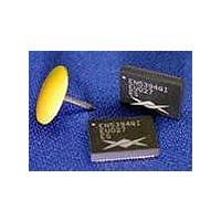
EN5364QI-E Enpirion, EN5364QI-E Datasheet - Page 2

EN5364QI-E
Manufacturer Part Number
EN5364QI-E
Description
Power Management Modules & Development Tools Eval Bd 6A Syn Buck PWM DC-DC Converter
Manufacturer
Enpirion
Type
DC/DC Switching Converters, Regulators & Controllersr
Datasheet
1.EN5364QI-E.pdf
(10 pages)
Specifications of EN5364QI-E
Input Voltage
2.375 V to 6.6 V
Output Voltage
0.6 V
Maximum Operating Temperature
+ 85 C
Minimum Operating Temperature
- 40 C
Product
Power Management Modules
For Use With/related Products
EN5364QI
Lead Free Status / RoHS Status
Lead free / RoHS Compliant
Available stocks
Company
Part Number
Manufacturer
Quantity
Price
Company:
Part Number:
EN5364QI-E
Manufacturer:
ST
Quantity:
34 000
Company:
Part Number:
EN5364QI-E
Manufacturer:
Enpirion
Quantity:
135
• The EN53x4QI features a customer programmable output voltage by
• The EN53x4QI includes the bulk of the compensation network internally.
• MAR1 and MAR2 are ternary input signals. The pins are allowed to be in a
• A footprint is provided for a SMC connector (not populated) for S_IN. A
means of a resistor divider. The resistor divider allows the user to set the
V
`Referring to Figure 1, the evaluation board, as shipped is populated with
a single R
one of the 4 R
1.8Volts. You can populate more than one R
higher output voltages. See “VOUT Programming” section in the
evaluation board schematic (Figure 7).
However, an external phase-lead (zero) capacitor is required as part of the
feedback. This network is shown in Figure -1. Appropriate component
values allow for optimum compensation for a given Input voltage and
choice of loop bandwidth. The equations in Figure 1 provide the details to
calculate component values.
low state (tied to GND), a high state (tied to V
shows the margining truth table. Accordingly, the output voltage can be
nominal or ±2.5%, ±5% or ±10% about the nominal. 7 out of 9 possible
states of MAR[1:2] are used for margining. The other two states are
reserved for diagnostics. If tying MAR[1,2] to V
recommended to reduce the pin input current (see Figure 2).
clock source (3.6 to 4.4MHz) may be applied to S_IN to synchronize the
device switching frequency to the external source. S_OUT will output a
clock signal synchronous with the switching frequency, with a phase
delay. S_OUT of one EN53x4QI may be connected to S_IN of another
EN53x4QI device in different modes of operation.
OUT
o
o
to any value within the range 0.6V to approximately (V
voltage may be coupled to the output via a diode. This diode (D2) is
populated on the board. Back-feed voltage may be applied at
BF_IN (TP18)
Parallel Mode operation
operated in parallel when load currents greater than 6A/9A is
desired. In parallel mode, one device is designated the Master and
up to 3 devices operate in slave mode, controlled by the Master.
The PWM output of the Master is routed to slave devices. By daisy
chaining the Slave devices even more devices can be operated in
parallel but practical considerations, such as board layout would
limit the number of slave devices to three.
Soft-Start
evaluation board for an output voltage ramp time of ~1ms. This may
be swapped for a different value capacitor if a different ramp time is
desired. To limit the inrush current this capacitor value should be
greater than 4.7nF. The output voltage rise time is ~65k*C
A
, a single C
B
resistors to produce a voltage of 0.804, 0.998, 1.2 or
– A 15nF (C11) soft-start capacitor is populated on the
EN5364QI-EN5394QI Evaluation Board Application Note
A
, and four possible R
Page 2 of 10
– Up to 4 EN53x4QI devices may be
B
B
IN
resistors. A jumper selects
jumper position to get even
IN
), or a float state. Table-1
, a series resistor is
November 2009 V_3
IN
-0.5V).
SS
.


