BLF369,112 NXP Semiconductors, BLF369,112 Datasheet
BLF369,112
Specifications of BLF369,112


Related parts for BLF369,112


BLF369,112 Summary of contents
Page 1
BLF369 Multi-use VHF power LDMOS transistor Rev. 04 — 19 February 2009 1. Product profile 1.1 General description A general purpose 500 W LDMOS RF power transistor for pulsed and continuous wave applications in the HF/VHF band up to 500 ...
Page 2
... NXP Semiconductors 1.3 Applications I Pulsed applications up to 500 MHz I Communication transmitter applications in the HF/VHF/UHF band under specific conditions I Industrial applications up to 500 MHz under special conditions 2. Pinning information Table 2. Pin [1] Connected to flange. 3. Ordering information Table 3. Type number BLF369 4. Limiting values Table 4 ...
Page 3
... NXP Semiconductors 5. Thermal characteristics Table 5. Symbol R th(j-case) R th(j-h) Z th(j-h) [ the junction temperature. j [2] R th(j-case) [3] R th(j-h) [4] See Figure 0.4 Z th(j-h) (7) (K/W) 0.3 0.2 (6) (3) (2) 0.1 (1) ( (7) = 100 % (DC) Fig 1. Transient thermal impedance from junction to heatsink as function of pulse duration BLF369_4 Product data sheet ...
Page 4
... NXP Semiconductors 6. Characteristics Table 6. Characteristics unless otherwise specified. j Symbol Parameter V drain-source breakdown voltage (BR)DSS V gate-source threshold voltage GS(th) I drain leakage current DSS I drain cut-off current DSX I gate leakage current GSS g forward transconductance fs R drain-source on-state resistance DS(on) C input capacitance iss ...
Page 5
... NXP Semiconductors 7. Application information Table 7. RF performance in a common-source 225 MHz test circuit unless otherwise specified. h Mode of operation f (MHz) CW, class AB 225 2-tone, class 225 [1] pulsed, class AB 225 [ ms 7.1 CW Fig 3. BLF369_4 Product data sheet (V) ( 1.0 500 = 225 1 (dB 100 200 CW power gain and drain efficiency as a function of output power; typical values Rev. 04 — ...
Page 6
... NXP Semiconductors 7.2 2-Tone (dB 200 225 MHz 1 Fig 4. 2-Tone power gain and drain efficiency as a function of peak envelope power; typical values 7.3 Pulsed (dB 200 400 f = 225 MHz Fig 6. Pulsed power gain as function of load power; typical values BLF369_4 Product data sheet 001aae502 ...
Page 7
... NXP Semiconductors (dB 200 400 f = 225 MHz Fig 8. Pulsed power gain as function of load power; typical values 7.4 Maximum heatsink temperature The heatsink temperature is defined 1 mm below the surface of the heatsink at the center of the flange. The maximum allowable heatsink temperature is given in the following graphs at several pulsed conditions as well as for CW ...
Page 8
... NXP Semiconductors 100 200 400 600 = 100 ms p Fig 10. Heatsink temperature as function of power dissipation at a duty cycle Fig 12. CW heatsink temperature as function of power dissipation 7.5 Ruggedness in class-AB operation The BLF369 is capable of withstanding a load mismatch corresponding to VSWR = through all phases under the following conditions: 2-tone signal; V ...
Page 9
... NXP Semiconductors 7.6 Reliability 6 10 Years ( TTF (0.1 % failure fraction); best estimate values. The reliability at pulsed conditions can be calculated as follows: TTF (0 100 110 120 130 140 150 160 170 180 C j (10 190 C ...
Page 10
... NXP Semiconductors Table 8. List of components For test circuit, see Figure 14, Figure 15 Component Description C20 multilayer ceramic chip capacitor C21 multilayer ceramic chip capacitor C22, C25 multilayer ceramic chip capacitor C23, C26 ceramic capacitor C24, C27 electrolytic capacitor C28, C31 multilayer ceramic chip capacitor ...
Page 11
C30 R11 C29 C28 50 B2 C31 R12 C32 C33 Fig 14. Class-AB common-source 225 MHz test circuit G1(test D1(test) C24 R7 C6 C23 C5 C22 C21 C20 ...
Page 12
Fig 15. Printed-Circuit Board (PCB) for class-AB 225 MHz test circuit 95 mm 001aae536 ...
Page 13
V G1(test) C30 R11 C29 C28 C31 C32 R12 B2 C33 + V G2(test) C1 mounted on top of transformers T1 and T2; C20 mounted on top of transformers T3 and T4. Fig 16. Component layout for class-AB 225 ...
Page 14
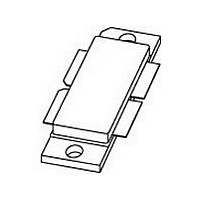
... NXP Semiconductors 9. Package outline Flanged LDMOST ceramic package; 2 mounting holes; 4 leads DIMENSIONS (millimetre dimensions are derived from the original inch dimensions) UNIT 6.3 10.55 0.15 30.5 mm 5.9 10.45 0.10 29.9 0.248 0.415 0.006 1.201 inches 0.232 0.411 0.004 1.177 OUTLINE VERSION ...
Page 15
... NXP Semiconductors 10. Abbreviations Table 9. Acronym CW DC GSM HF LDMOS LDMOST PEP RF TTF UHF VHF VSWR 11. Revision history Table 10. Revision history Document ID Release date BLF369_4 20090219 • Modifications: Data sheet status updated from 'Preliminary data sheet' to 'Product data sheet' BLF369_3 20080129 BLF369_2 ...
Page 16
... Right to make changes — NXP Semiconductors reserves the right to make changes to information published in this document, including without limitation specifications and product descriptions, at any time and without notice ...
Page 17
... NXP Semiconductors 14. Contents 1 Product profi 1.1 General description 1.2 Features . . . . . . . . . . . . . . . . . . . . . . . . . . . . . . 1 1.3 Applications . . . . . . . . . . . . . . . . . . . . . . . . . . . 2 2 Pinning information . . . . . . . . . . . . . . . . . . . . . . 2 3 Ordering information . . . . . . . . . . . . . . . . . . . . . 2 4 Limiting values Thermal characteristics Characteristics . . . . . . . . . . . . . . . . . . . . . . . . . . 4 7 Application information 7 7.2 2-Tone 7.3 Pulsed 7.4 Maximum heatsink temperature . . . . . . . . . . . . 7 7.5 Ruggedness in class-AB operation 7.6 Reliability ...