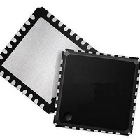
ispPAC-POWR607-01SN32I Lattice, ispPAC-POWR607-01SN32I Datasheet - Page 14

ispPAC-POWR607-01SN32I
Manufacturer Part Number
ispPAC-POWR607-01SN32I
Description
Supervisory Circuits Prec Prog Pwr Supply Seq Mon IND
Manufacturer
Lattice
Type
Power Supply Sequencer and Monitorr
Series
ispPAC®r
Datasheet
1.ISPPAC-POWR607-01SN32I.pdf
(28 pages)
Specifications of ispPAC-POWR607-01SN32I
Internal Hysteresis
Yes
Minimum Operating Temperature
- 40 C
Output Type
Open Collector / Drain
Power Fail Detection
Yes
Number Of Voltages Monitored
6
Monitored Voltage
Adj V
Undervoltage Threshold
Adj
Overvoltage Threshold
Adj
Manual Reset
Resettable
Watchdog
Yes
Power-up Reset Delay (typ)
100 us
Supply Voltage (max)
3.96 V
Supply Voltage (min)
2.64 V
Supply Current (typ)
3.5 mA
Mounting Style
SMD/SMT
Maximum Operating Temperature
+ 85 C
Package / Case
QFN-32
Applications
General Purpose
Voltage - Input
-0.3 V ~ 5.9 V
Voltage - Supply
2.64 V ~ 3.96 V
Current - Supply
3.5mA
Operating Temperature
-40°C ~ 85°C
Mounting Type
Surface Mount
Lead Free Status / RoHS Status
Lead free / RoHS Compliant
Available stocks
Company
Part Number
Manufacturer
Quantity
Price
Company:
Part Number:
ISPPAC-POWR607-01SN32I
Manufacturer:
LATTICE
Quantity:
284
Part Number:
ISPPAC-POWR607-01SN32I
Manufacturer:
LATTICE
Quantity:
20 000
Lattice Semiconductor
Figure 4-10. ispPAC-POWR607 PLD Architecture
Macrocell Architecture
The macrocell shown in Figure 4-11 is the heart of the PLD. The basic macrocell has five product terms that feed
the OR gate and the flip-flop. The flip-flop in each macrocell is independently configured. It can be programmed to
function as a D-Type or T-Type flip-flop. Combinatorial functions are realized by bypassing the flip-flop. The polarity
control and XOR gates provide additional flexibility for logic synthesis. The flip-flop’s clock is driven from the com-
mon PLD clock that is generated by dividing the 8 MHz master clock (MCLK) by 32. The macrocell also supports
asynchronous reset and preset functions, derived from either product terms or the power-on reset signal. The
resources within the macrocells share routing and contain a product term allocation array. The product term alloca-
tion array greatly expands the PLD’s ability to implement complex logical functions by allowing logic to be shared
between adjacent blocks and distributing the product terms to allow for wider decode functions. All the digital inputs
are registered by MCLK and all VMON comparator outputs are registered using the PLD Clock to synchronize them
to the PLD logic as shown in Figure 4-10.
IN1_PWRDN
IN2
IN_OUT[3:7]
VMON[1:6]
VCC
Sleep/
Wake
Logic
Output
Feedback
Timer0
Timer1
Timer2
Timer3
5
6
4
Register
Register
MCLK
Input
Input
16
R
P
I
81 P-Terms
PLD Clock
AND Array
28 Inputs
16
PLD_PWRDN
4-14
16
81
Reset
16 Macrocell
Timer Clock
81 P-Terms
Generic
Logic
Block
GLB
ispPAC-POWR607 Data Sheet
HVOUT[1:2]
IN_OUT[3:7]


