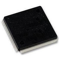
LFXP2-5E-5QN208C Lattice, LFXP2-5E-5QN208C Datasheet - Page 10

LFXP2-5E-5QN208C
Manufacturer Part Number
LFXP2-5E-5QN208C
Description
FPGA - Field Programmable Gate Array 5K LUTs 146I/O Inst- on DSP 1.2V -5 Spd
Manufacturer
Lattice
Datasheet
1.LFXP2-40E-5FN484I.pdf
(92 pages)
Specifications of LFXP2-5E-5QN208C
Number Of Macrocells
5000
Maximum Operating Frequency
200 MHz
Number Of Programmable I/os
146
Data Ram Size
10 KB
Supply Voltage (max)
1.14 V
Supply Current
17 mA
Maximum Operating Temperature
+ 85 C
Minimum Operating Temperature
0 C
Mounting Style
SMD/SMT
Supply Voltage (min)
1.26 V
Package / Case
PQFP-208
Lead Free Status / RoHS Status
Lead free / RoHS Compliant
Available stocks
Company
Part Number
Manufacturer
Quantity
Price
Company:
Part Number:
LFXP2-5E-5QN208C
Manufacturer:
Lattice Semiconductor Corporation
Quantity:
10 000
Part Number:
LFXP2-5E-5QN208C
Manufacturer:
LATTICE
Quantity:
20 000
Lattice Semiconductor
Figure 2-4. General Purpose PLL (GPLL) Diagram
Table 2-4 provides a description of the signals in the GPLL blocks.
Table 2-4. GPLL Block Signal Descriptions
Clock Dividers
LatticeXP2 devices have two clock dividers, one on the left side and one on the right side of the device. These are
intended to generate a slower-speed system clock from a high-speed edge clock. The block operates in a ÷2, ÷4 or
÷8 mode and maintains a known phase relationship between the divided down clock and the high-speed clock
based on the release of its reset signal. The clock dividers can be fed from the CLKOP output from the GPLLs or
from the Edge Clocks (ECLK). The clock divider outputs serve as primary clock sources and feed into the clock dis-
tribution network. The Reset (RST) control signal resets the input and forces all outputs to low. The RELEASE sig-
nal releases outputs to the input clock. For further information on clock dividers, please see TN1126,
sysCLOCK PLL Design and Usage
CLKI
CLKFB
RST
RSTK
DPHASE [3:0]
DDDUTY [3:0]
WRDEL
CLKOS
CLKOP
CLKOK
CLKOK2
LOCK
DPHASE
WRDEL
DDUTY
CLKFB
RSTK
Signal
CLKI
RST
I/O
O
O
O
O
O
I
I
I
I
I
I
I
Clock input from external pin or routing
DPA Phase Adjust input
DPA Duty Cycle Select input
PLL feedback input from CLKOP (PLL internal), from clock net (CLKOP) or from a user clock
(PIN or logic)
“1” to reset PLL counters, VCO, charge pumps and M-dividers
“1” to reset K-divider
DPA Fine Delay Adjust input
PLL output clock to clock tree (phase shifted/duty cycle changed)
PLL output clock to clock tree (no phase shift)
PLL output to clock tree through secondary clock divider
PLL output to clock tree (CLKOP divided by 3)
“1” indicates PLL LOCK to CLKI
CLKFB
Divider
Divider
CLKI
Guide. Figure 2-5 shows the clock divider connections.
Internal Feedback
PFD
LOOP FILTER
2-7
VCO/
Description
CLKOP
Divider
Detect
Lock
LatticeXP2 Family Data Sheet
Duty Cycle/
Duty Trim
Duty Trim
CLKOK
Phase/
Divider
3
Architecture
LatticeXP2
CLKOK2
CLKOS
CLKOP
CLKOK
LOCK


