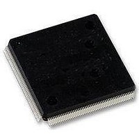
LFXP2-5E-5QN208C Lattice, LFXP2-5E-5QN208C Datasheet - Page 21

LFXP2-5E-5QN208C
Manufacturer Part Number
LFXP2-5E-5QN208C
Description
FPGA - Field Programmable Gate Array 5K LUTs 146I/O Inst- on DSP 1.2V -5 Spd
Manufacturer
Lattice
Datasheet
1.LFXP2-40E-5FN484I.pdf
(92 pages)
Specifications of LFXP2-5E-5QN208C
Number Of Macrocells
5000
Maximum Operating Frequency
200 MHz
Number Of Programmable I/os
146
Data Ram Size
10 KB
Supply Voltage (max)
1.14 V
Supply Current
17 mA
Maximum Operating Temperature
+ 85 C
Minimum Operating Temperature
0 C
Mounting Style
SMD/SMT
Supply Voltage (min)
1.26 V
Package / Case
PQFP-208
Lead Free Status / RoHS Status
Lead free / RoHS Compliant
Available stocks
Company
Part Number
Manufacturer
Quantity
Price
Company:
Part Number:
LFXP2-5E-5QN208C
Manufacturer:
Lattice Semiconductor Corporation
Quantity:
10 000
Part Number:
LFXP2-5E-5QN208C
Manufacturer:
LATTICE
Quantity:
20 000
Lattice Semiconductor
For further information on the sysMEM EBR block, please see TN1137,
EBR Asynchronous Reset
EBR asynchronous reset or GSR (if used) can only be applied if all clock enables are low for a clock cycle before the
reset is applied and released a clock cycle after the low-to-high transition of the reset signal, as shown in Figure 2-18.
The GSR input to the EBR is always asynchronous.
Figure 2-18. EBR Asynchronous Reset (Including GSR) Timing Diagram
If all clock enables remain enabled, the EBR asynchronous reset or GSR may only be applied and released after
the EBR read and write clock inputs are in a steady state condition for a minimum of 1/f
release must adhere to the EBR synchronous reset setup time before the next active read or write clock edge.
If an EBR is pre-loaded during configuration, the GSR input must be disabled or the release of the GSR during
device Wake Up must occur before the release of the device I/Os becoming active.
These instructions apply to all EBR RAM and ROM implementations.
Note that there are no reset restrictions if the EBR synchronous reset is used and the EBR GSR input is disabled.
sysDSP™ Block
The LatticeXP2 family provides a sysDSP block making it ideally suited for low cost, high performance Digital Sig-
nal Processing (DSP) applications. Typical functions used in these applications include Bit Correlators, Fast Fourier
Transform (FFT) functions, Finite Impulse Response (FIR) Filter, Reed-Solomon Encoder/Decoder, Turbo Encoder/
Decoder and Convolutional Encoder/Decoder. These complex signal processing functions use similar building
blocks such as multiply-adders and multiply-accumulators.
sysDSP Block Approach Compare to General DSP
Conventional general-purpose DSP chips typically contain one to four (Multiply and Accumulate) MAC units with
fixed data-width multipliers; this leads to limited parallelism and limited throughput. Their throughput is increased by
higher clock speeds. The LatticeXP2 family, on the other hand, has many DSP blocks that support different data-
widths. This allows the designer to use highly parallel implementations of DSP functions. The designer can opti-
mize the DSP performance vs. area by choosing appropriate levels of parallelism. Figure 2-19 compares the fully
serial and the mixed parallel and serial implementations.
Reset
Clock
Clock
Enable
2-18
LatticeXP2 Memory Usage
LatticeXP2 Family Data Sheet
MAX
(EBR clock). The reset
Architecture
Guide.


