NTE457 NTE ELECTRONICS, NTE457 Datasheet
NTE457
Manufacturer Part Number
NTE457
Description
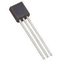
Replacement Semiconductors TO-92 N-CHAN JFET
Manufacturer
NTE ELECTRONICS
Datasheet
1.NTE457.pdf
(2 pages)
Specifications of NTE457
Transistor Type
JFET
Breakdown Voltage Vbr
-25V
Gate-source Cutoff Voltage Vgs(off) Max
6V
Power Dissipation Pd
310mW
No. Of Pins
3
Current Rating
5mA
Voltage Rating
-25V
Lead Free Status / RoHS Status
Lead free / RoHS Compliant
Lead Free Status / RoHS Status
Lead free / RoHS Compliant, Lead free / RoHS Compliant


Absolute Maximum Ratings:
Drain–Source Voltage, V
Drain–Gate Voltage, V
Reverse Gate–Source Voltage, V
Gate Current, I
Total Device Dissipation (T
Operating Junction Temperature, T
Storage Temperature Range, T
Electrical Characteristics: (T
Note 1. Pulse Test: Pulse Width
OFF Characteristics
Gate–Source Breakdown Voltage
Gate Reverse Current
Gate–Source Cutoff Voltage
Gate–Source Voltage
ON Characteristics
Zero–Gate Voltage Drain Current
Small–Signal Characteristics
Forward Transfer Admittance
Output Admittance Common Source
Input Capacitance
Reverse Transfer Capacitance
Common Source
Derate Above 25 C
Parameter
G
. . . . . . . . . . . . . . . . . . . . . . . . . . . . . . . . . . . . . . . . . . . . . . . . . . . . . . . . . . . . . . . . . .
DG
Silicon N–Channel JFET Transistor
DS
. . . . . . . . . . . . . . . . . . . . . . . . . . . . . . . . . . . . . . . . . . . . . . . . . . . . . . . . . . . .
A
. . . . . . . . . . . . . . . . . . . . . . . . . . . . . . . . . . . . . . . . . . . . . . . . . . . .
General Purpose Amp, Switch
. . . . . . . . . . . . . . . . . . . . . . . . . . . . . . . . . . . . . . . . . . . . . . . . . . . . . . . . . .
= +25 C), P
stg
A
= +25 C unless otherwise specified)
GSR
Symbol
J
V
. . . . . . . . . . . . . . . . . . . . . . . . . . . . . . . . . . . . . . . . . .
V
630ms, Duty Cycle
(BR)GS
I
I
GS(off)
V
|y
C
C
|y
GSS
DSS
. . . . . . . . . . . . . . . . . . . . . . . . . . . . . . . . . . . . . . . . . . . . . . .
S
GS
os
rss
iss
fs
. . . . . . . . . . . . . . . . . . . . . . . . . . . . . . . . . . . . . . . . . . . . . . . .
|
|
D
. . . . . . . . . . . . . . . . . . . . . . . . . . . . . . . . . . . . . . . . .
I
V
V
V
V
V
V
Note 1
V
Note 1
V
V
NTE457
G
GS
GS
DS
DS
DS
DS
DS
DS
DS
= –10 A, V
= 15V, I
= 15V, I
= 15V, V
= 15V, V
= 15V, V
= 15V, V
= 15V, V
= 15V, V
= 15V, V
Test Conditions
D
D
GS
GS
GS
GS
GS
DS
DS
DS
= 10nA
= 100 A
= 0
= 0, T
= 0, Note 1
= 0, f = 1kHz,
= 0, f = 1kHz,
= 0, f = 1kHz
= 0, f = 1kHz
10%.
= 0
A
= +100 C
1000
–0.5
Min
–25
–
–
–
1
–
–
–
Typ
4.5
1.5
10
–
–
–
–
–
3
–
–65 to +150 C
–200
5000
Max
–6.0
–2.5
7.0
3.0
–1
50
2.82mW/ C
–
5
310mW
+125 C
10mA
Unit
mhos
mhos
mA
mA
mA
–25V
pF
pF
V
V
V
25V
25V
Related parts for NTE457
Image
Part Number
Description
Manufacturer
Datasheet
Request
R

Part Number:
Description:
TRANSISTOR,BJT,PAIR,PNP,100V V(BR)CEO,100MA I(C),SIP
Manufacturer:
NTE ELECTRONICS

Part Number:
Description:
ICS,NTE LED FLASHLIGHTS,ICS,RED TRAFFIC AND SAFETY WAND FOR LW-PRO4000-BLK. MOLDED TRANSLUCENT PLASTIC WAND,TASK LIGHTING,LIGHTWAVE? LED FLASHLIGHTS ,NTE ELECTRONICS
Manufacturer:
NTE ELECTRONICS

Part Number:
Description:
Fuse; Non-Resettable; 15A; Dims 0.16x0.457"; Axial; 120-277VAC; PCB; NTE Series
Manufacturer:
NTE Electronics, Inc.
Datasheet:
Part Number:
Description:
Fuse; Non-Resettable; 15A; Dims 0.16x0.457"; Axial; 120-277VAC; PCB; NTE Series
Manufacturer:
NTE Electronics, Inc.
Datasheet:
Part Number:
Description:
Fuse; Non-Resettable; 15A; Dims 0.16x0.457"; Axial; 120-277VAC; PCB; NTE Series
Manufacturer:
NTE Electronics, Inc.
Datasheet:
Part Number:
Description:
Fuse; Non-Resettable; 15A; Dims 0.16x0.457"; Axial; 120-277VAC; PCB; NTE Series
Manufacturer:
NTE Electronics, Inc.
Datasheet:
Part Number:
Description:
Fuse; Non-Resettable; 15A; Dims 0.16x0.457"; Axial; 120-277VAC; PCB; NTE Series
Manufacturer:
NTE Electronics, Inc.
Datasheet:
Part Number:
Description:
Fuse; Non-Resettable; 15A; Dims 0.16x0.457"; Axial; 120-277VAC; PCB; NTE Series
Manufacturer:
NTE Electronics, Inc.
Datasheet:
Part Number:
Description:
Fuse; Non-Resettable; 15A; Dims 0.16x0.457"; Axial; 120-277VAC; PCB; NTE Series
Manufacturer:
NTE Electronics, Inc.
Datasheet:
Part Number:
Description:
Fuse; Non-Resettable; 15A; Dims 0.16x0.457"; Axial; 120/250VAC; PCB; NTE Series
Manufacturer:
NTE Electronics, Inc.
Datasheet:
Part Number:
Description:
MOTOR START AC ELECTROLYTIC
Manufacturer:
NTE [NTE Electronics]
Datasheet:
Part Number:
Description:
SOLID TANTALUM
Manufacturer:
NTE [NTE Electronics]
Datasheet:
Part Number:
Description:
HIGH-FREQ ALUMINUM ELECTROLYTIC
Manufacturer:
NTE [NTE Electronics]
Datasheet:
Part Number:
Description:
SNAP-IN MOUNT ALUMINUM ELECTROLYTIC
Manufacturer:
NTE [NTE Electronics]
Datasheet:

Part Number:
Description:
Replacement Semiconductors TO-220 NPN PWR AMP
Manufacturer:
NTE ELECTRONICS
Datasheet:
NTE457 Summary of contents
Page 1
... Reverse Transfer Capacitance Note 1. Pulse Test: Pulse Width NTE457 General Purpose Amp, Switch . . . . . . . . . . . . . . . . . . . . . . . . . . . . . . . . . . . . . . . . . . . . . . . . . . . . . . . . . . ...
Page 2
Max .500 (12.7) Min .100 (2.54) .105 (2.67) Max .205 (5.2) Max .135 (3.45) Min Seating Plane .021 (.445) Dia Max .050 (1.27) .165 (4.2) Max .105 (2.67) Max ...