NTE929 NTE ELECTRONICS, NTE929 Datasheet
NTE929
Manufacturer Part Number
NTE929
Description
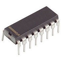
Replacement Semiconductors DIP-16 GP TRAN ARRAY
Manufacturer
NTE ELECTRONICS
Datasheet
1.NTE929.pdf
(2 pages)
Specifications of NTE929
Transistor Polarity
NPN
Collector Emitter Voltage V(br)ceo
15V
Transition Frequency Typ Ft
450MHz
Power Dissipation Pd
750mW
Dc Collector Current
20mA
Dc Current Gain Hfe
40
Lead Free Status / RoHS Status
Lead free / RoHS Compliant
Lead Free Status / RoHS Status
Lead free / RoHS Compliant


Description:
The NTE929 is a versatile array of five high–current (to 100mA) NPN transistors on a common mono-
lithic substrate. In addition, two of these transistors (Q1 and Q2) are matched at low currents (i.e.
1mA) for applications in which offset parameters are of special importance.
Independent connections for each transistors plus a separate terminal for the substrate permit maxi-
mum flexibility in circuit design.
Features:
D High I
D Low V
D Matched pair (Q1 and Q2)
D 5 independent transistors plus separate substrate connection.
Applications:
D Signal processing and switching systems operating from DC to VHF
D Lamp and relay driver
D Differential amplifier
D Temperature–compensated amplifier
D Thyristor firing
Absolute Maximum Ratings: (T
Power Dissipation, P
Operating Ambient Temperature Range, T
Storage Temperature range, T
Lead Temperature (During Soldering, 1/16” 1/32” from case, 10sec max), T
The following ratings apply for each transistor in the device:
Collector–Emitter Voltage, V
Collector–Base Voltage, V
Collector–Substrate Voltage, V
Emitter–Base Voltage, V
Collector Current, I
Base Current, I
Note 1. The collector of each transistor of the NTE929 is isolated from the substrate by an integral
Any One Transistor
Total Package
diode. The substrate must be connected to a voltage which is more negative than any collec-
tor voltage in order to maintain isolation between transistors and provide normal transistor
action. To avoid undesired coupling between transistors, the substrate terminal (Pin5)
should be maintained at either DC or signal (AC) ground. A suitable bypass capacitor can
be used to establish a signal ground.
C
CEsat
V
I
Derate Above 55 C
10
General Purpose, High Current, NPN Transistor Array
100mA max
10
(at 1mA): 2.5 A max.
(V
(at 50mA) 0.7V max.
B
BE
. . . . . . . . . . . . . . . . . . . . . . . . . . . . . . . . . . . . . . . . . . . . . . . . . . . . . . . . . . . . . . . . .
C
matched):
D
. . . . . . . . . . . . . . . . . . . . . . . . . . . . . . . . . . . . . . . . . . . . . . . . . . . . . . . . . . . . . .
. . . . . . . . . . . . . . . . . . . . . . . . . . . . . . . . . . . . . . . . . . . . . . . . . . . . . . . . . . .
EBO
CBO
. . . . . . . . . . . . . . . . . . . . . . . . . . . . . . . . . . . . . . . . . . . . . . . . . . . . . . .
CEO
. . . . . . . . . . . . . . . . . . . . . . . . . . . . . . . . . . . . . . . . . . . . . . . . . . . . . . . . . .
stg
. . . . . . . . . . . . . . . . . . . . . . . . . . . . . . . . . . .
CIO
. . . . . . . . . . . . . . . . . . . . . . . . . . . . . . . . . . . . . . . . . . . . . . . . . . . . . . .
5mV max.
. . . . . . . . . . . . . . . . . . . . . . . . . . . . . . . . . . . . . . . . . . . . . . . . . . . . . .
A
. . . . . . . . . . . . . . . . . . . . . . . . . . . . . . . . . . . . . . . . . . .
. . . . . . . . . . . . . . . . . . . . . . . . . . . . . . . . . . . . . . . . . . . . . . . . . . . .
= +25 C unless otherwise specified)
Integrated Circuit
opr
NTE929
. . . . . . . . . . . . . . . . . . . . . . . . . . . . . . . . .
Derate Linearly 6.67mW/ C
L
. . . . . . . . . . .
–55 to +125 C
–65 to +150 C
500mW
750mW
+265 C
20mA
20mA
15V
20V
20V
5V
Related parts for NTE929
Image
Part Number
Description
Manufacturer
Datasheet
Request
R

Part Number:
Description:
TRANSISTOR,BJT,NPN,200V V(BR)CEO,15A I(C),SIP
Manufacturer:
NTE ELECTRONICS
Datasheet:
Part Number:
Description:
Silicon Complementary Transistors Hi-Fi Power Amp / Audio Ourtput
Manufacturer:
NTE Electronics
Datasheet:

Part Number:
Description:
ICS,NTE LED FLASHLIGHTS,ICS,RED TRAFFIC AND SAFETY WAND FOR LW-PRO4000-BLK. MOLDED TRANSLUCENT PLASTIC WAND,TASK LIGHTING,LIGHTWAVE? LED FLASHLIGHTS ,NTE ELECTRONICS
Manufacturer:
NTE ELECTRONICS

Part Number:
Description:
Fuse; Non-Resettable; 15A; Dims 0.16x0.457"; Axial; 120-277VAC; PCB; NTE Series
Manufacturer:
NTE Electronics, Inc.
Datasheet:
Part Number:
Description:
Fuse; Non-Resettable; 15A; Dims 0.16x0.457"; Axial; 120-277VAC; PCB; NTE Series
Manufacturer:
NTE Electronics, Inc.
Datasheet:
Part Number:
Description:
Fuse; Non-Resettable; 15A; Dims 0.16x0.457"; Axial; 120-277VAC; PCB; NTE Series
Manufacturer:
NTE Electronics, Inc.
Datasheet:
Part Number:
Description:
Fuse; Non-Resettable; 15A; Dims 0.16x0.457"; Axial; 120-277VAC; PCB; NTE Series
Manufacturer:
NTE Electronics, Inc.
Datasheet:
Part Number:
Description:
Fuse; Non-Resettable; 15A; Dims 0.16x0.457"; Axial; 120-277VAC; PCB; NTE Series
Manufacturer:
NTE Electronics, Inc.
Datasheet:
Part Number:
Description:
Fuse; Non-Resettable; 15A; Dims 0.16x0.457"; Axial; 120-277VAC; PCB; NTE Series
Manufacturer:
NTE Electronics, Inc.
Datasheet:
Part Number:
Description:
Fuse; Non-Resettable; 15A; Dims 0.16x0.457"; Axial; 120-277VAC; PCB; NTE Series
Manufacturer:
NTE Electronics, Inc.
Datasheet:
Part Number:
Description:
Fuse; Non-Resettable; 15A; Dims 0.16x0.457"; Axial; 120/250VAC; PCB; NTE Series
Manufacturer:
NTE Electronics, Inc.
Datasheet:
Part Number:
Description:
NTE Zener Diode, Nominal Zener Voltage: 6.8 V, Zener Test Current: 5 MA, Reverse Current: 100 NA AT 3 V, Typical Differential Resistance: 8 Ohm, Typical Temperature Coefficient: 3 MV/K, Typical Diode Capacitance: 105 PF
Manufacturer:
NTE ELECTRONICS
Part Number:
Description:
NTE Zener Diode, Nominal Zener Voltage: 12 V, Zener Test Current: 5 MA, Reverse Current: 100 NA AT .7 VZnom, Typical Differential Resistance: 10 Ohm, Typical Temperature Coefficient: 8.4 MV/K, Typical Diode Capacitance: 65 PF
Manufacturer:
NTE ELECTRONICS
Part Number:
Description:
NTE Industrial Rectifier, Peak Reverse Voltage: 50 V, Maximum Average Rectified Forward Current, IF: 12 A, IFSM: 250 A, VF AT IF: 1.2 V Max AT 1V Typ
Manufacturer:
NTE ELECTRONICS
NTE929 Summary of contents
Page 1
... B Note 1. The collector of each transistor of the NTE929 is isolated from the substrate by an integral diode. The substrate must be connected to a voltage which is more negative than any collec- tor voltage in order to maintain isolation between transistors and provide normal transistor action ...
Page 2
Electrical Characteristics: (T Parameter For Each Transistor Collector–Base Breakdown Voltage Collector–Emitter Breakdown Voltage Collector–Substrate Breakdown Voltage Emitter–Base Breakdown Voltage Collector Cutoff Current DC Forward Current Base–Emitter Voltage Collector–Emitter Saturation Voltage Gain–Bandwidth Product Absolute Input Offset Voltage Absolute Input Offset Current ...