Description:
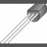
The NTE950, NTE951, and NTE977 are positive 3–terminal voltage regulators in available in a TO92
type package. With adequate heat sinking these regulators can deliver 100mA output current. Cur-
rent limiting is included to limit peak output current to safe value. Safe area protection for the output
transistors is provided to limit internal power dissipation. If internal power dissipation becomes too
high for the heat sinking provided, the thermal shutdown circuit takes over preventing the IC from
overheating.
When used as a zener diode/resistor combination replacement, these devices usually result in an ef-
fective output impedance improvement of two orders of magnitude, and lower quiescent current.
These regulators can provide local on card regulation, eliminating the distribution problems
associated with single point regulation. Typical applications include use in logic systems, instrumen-
tation, HiFi, and other solid state electronic equipment. Although designed primarily as fixed voltage
regulators these devices can be used with external components to obtain adjustment voltages and
currents.
Features:
D Output Voltage Tolerances of 5% over the Temperature Range
D Output Current of 100mA
D Internal Thermal Overload Protection
D Output Transistor Safe Area Protection
D Internal Short Circuit Current Limit
Absolute Maximum Ratings:
Output Voltage, V
Input Voltage, V
Internal Power Dissipation (Note 1), P
Operating Temperature Range, T
Maximum Junction Temperature, T
Storage Temperature Range, T
Lead Temperature (Soldering, 10 sec), T
Note 1. Thermal resistance is typically +60 C/W junction to case, +232 C/W junction to ambient, and
NTE977
NTE950
NTE951
NTE977
NTE950, NTE951
+88 C/W junction to ambient at 400ft min of air. The maximum junction temperature shall
not exceed +125 C on Electrical parameters.
. . . . . . . . . . . . . . . . . . . . . . . . . . . . . . . . . . . . . . . . . . . . . . . . . . . . . . . . . . . . . . . . . . . . . .
. . . . . . . . . . . . . . . . . . . . . . . . . . . . . . . . . . . . . . . . . . . . . . . . . . . . . . . . . . . . . . . . . . . . .
. . . . . . . . . . . . . . . . . . . . . . . . . . . . . . . . . . . . . . . . . . . . . . . . . . . . . . . . . . . . . . . . . . . . .
. . . . . . . . . . . . . . . . . . . . . . . . . . . . . . . . . . . . . . . . . . . . . . . . . . . . . . . . . . . . . . . . . . . . .
IN
Positive 3 Terminal Voltage Regulator, 100mA
OUT
. . . . . . . . . . . . . . . . . . . . . . . . . . . . . . . . . . . . . . . . . . . . . . . . . . . . . . . . . . . .
stg
NTE950/NTE951/NTE977
opr
J
. . . . . . . . . . . . . . . . . . . . . . . . . . . . . . . . . . . . . . . .
Integrated Circuit
. . . . . . . . . . . . . . . . . . . . . . . . . . . . . . . . . . . . . . . . . .
. . . . . . . . . . . . . . . . . . . . . . . . . . . . . . . . . . . . . . . . . . . . . . .
D
L
. . . . . . . . . . . . . . . . . . . . . . . . . . . . . . . . . . .
. . . . . . . . . . . . . . . . . . . . . . . . . . . . . . . . . . . . . . . . . .
Internally Limited
–55 C to +150 C
0 C to +70 C
+125 C
+260 C
12V
15V
30V
35V
5V