PIC18F45K80-I/PT Microchip Technology, PIC18F45K80-I/PT Datasheet - Page 109
PIC18F45K80-I/PT
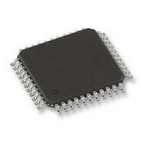
Manufacturer Part Number
PIC18F45K80-I/PT
Description
MCU PIC 32KB FLASH 44TQFP
Manufacturer
Microchip Technology
Series
PIC® XLP™ 18Fr
Datasheet
1.PIC18F25K80-ISO.pdf
(628 pages)
Specifications of PIC18F45K80-I/PT
Core Size
8-Bit
Program Memory Size
32KB (16K x 16)
Peripherals
Brown-out Detect/Reset, LVD, POR, PWM, WDT
Core Processor
PIC
Speed
64MHz
Connectivity
ECAN, I²C, LIN, SPI, UART/USART
Number Of I /o
35
Program Memory Type
FLASH
Eeprom Size
1K x 8
Ram Size
3.6K x 8
Voltage - Supply (vcc/vdd)
1.8 V ~ 5.5 V
Data Converters
A/D 11x12b
Oscillator Type
Internal
Operating Temperature
-40°C ~ 85°C
Package / Case
44-TQFP
Controller Family/series
PIC18
Ram Memory Size
4KB
Cpu Speed
16MIPS
No. Of Pwm Channels
5
Embedded Interface Type
I2C, SPI, USART
Processor Series
PIC18F45K80
Core
PIC
Data Bus Width
8 bit
Data Ram Size
1 KB
Interface Type
I2C, SPI, USART
Maximum Clock Frequency
64 MHz
Number Of Programmable I/os
35
Number Of Timers
5
Operating Supply Voltage
1.8 V to 5.5 V
Maximum Operating Temperature
+ 85 C
Mounting Style
SMD/SMT
Lead Free Status / RoHS Status
Lead free / RoHS Compliant
Lead Free Status / RoHS Status
Lead free / RoHS Compliant
Available stocks
Company
Part Number
Manufacturer
Quantity
Price
Company:

Part Number:
PIC18F45K80-I/PT
Manufacturer:
MICROCHIP
Quantity:
1 500
Company:
Part Number:
PIC18F45K80-I/PT
Manufacturer:
PIC
Quantity:
400
Company:
Part Number:
PIC18F45K80-I/PT
Manufacturer:
Microchip Technology
Quantity:
10 000
Part Number:
PIC18F45K80-I/PT
Manufacturer:
MICROCHIP/微芯
Quantity:
20 000


6.1.3.4
Device Resets on stack overflow and stack underflow
conditions are enabled by setting the STVREN bit
(CONFIG4L<0>). When STVREN is set, a full or under-
flow condition will set the appropriate STKFUL or
STKUNF bit and then cause a device Reset. When
STVREN is cleared, a full or underflow condition will set
the appropriate STKFUL or STKUNF bit, but not cause
a device Reset. The STKFUL or STKUNF bits are
cleared by the user software or a Power-on Reset.
6.1.4
A Fast Register Stack is provided for the STATUS,
WREG and BSR registers to provide a “fast return”
option for interrupts. This stack is only one level deep
and is neither readable nor writable. It is loaded with the
current value of the corresponding register when the
processor vectors for an interrupt. All interrupt sources
will push values into the Stack registers. The values in
the registers are then loaded back into the working
registers if the RETFIE , FAST instruction is used to
return from the interrupt.
If both low and high-priority interrupts are enabled, the
Stack registers cannot be used reliably to return from
low-priority interrupts. If a high-priority interrupt occurs
while servicing a low-priority interrupt, the Stack
register values stored by the low-priority interrupt will
be overwritten. In these cases, users must save the key
registers in software during a low-priority interrupt.
If interrupt priority is not used, all interrupts may use the
Fast Register Stack for returns from interrupt. If no
interrupts are used, the Fast Register Stack can be
used to restore the STATUS, WREG and BSR registers
at the end of a subroutine call. To use the Fast Register
Stack for a subroutine call, a CALL label , FAST
instruction must be executed to save the STATUS,
WREG and BSR registers to the Fast Register Stack. A
RETURN , FAST instruction is then executed to restore
these registers from the Fast Register Stack.
Example 6-1
the Fast Register Stack during a subroutine call and
return.
EXAMPLE 6-1:
2011 Microchip Technology Inc.
CALL SUB1, FAST
SUB1
RETURN FAST
FAST REGISTER STACK
shows a source code example that uses
Stack Full and Underflow Resets
FAST REGISTER STACK
CODE EXAMPLE
;STATUS, WREG, BSR
;SAVED IN FAST REGISTER
;STACK
;RESTORE VALUES SAVED
;IN FAST REGISTER STACK
Preliminary
PIC18F66K80 FAMILY
6.1.5
There may be programming situations that require the
creation of data structures, or look-up tables, in
program memory. For PIC18 devices, look-up tables
can be implemented in two ways:
• Computed GOTO
• Table Reads
6.1.5.1
A computed GOTO is accomplished by adding an offset
to the program counter. An example is shown in
Example
A look-up table can be formed with an ADDWF PCL
instruction and a group of RETLW nn instructions. The
W register is loaded with an offset into the table before
executing a call to that table. The first instruction of the
called routine is the ADDWF PCL instruction. The next
instruction executed will be one of the RETLW
instructions that returns the value, ‘ nn ’, to the calling
function.
The offset value (in WREG) specifies the number of
bytes that the program counter should advance and
should be multiples of two (LSb = 0 ).
In this method, only one data byte may be stored in
each instruction location and room on the return
address stack is required.
EXAMPLE 6-2:
6.1.5.2
A better method of storing data in program memory
allows two bytes of data to be stored in each instruction
location.
Look-up table data may be stored two bytes per
program word while programming. The Table Pointer
(TBLPTR) specifies the byte address and the Table
Latch (TABLAT) contains the data that is read from the
program memory. Data is transferred from program
memory one byte at a time.
The table read operation is discussed further in
Section 7.1 “Table Reads and Table Writes”
ORG
TABLE
6-2.
MOVF
CALL
nn00h
ADDWF
RETLW
RETLW
RETLW
.
.
.
LOOK-UP TABLES IN PROGRAM
MEMORY
Computed GOTO
Table Reads
OFFSET, W
TABLE
PCL
nnh
nnh
nnh
COMPUTED GOTO USING
AN OFFSET VALUE
DS39977C-page 109
.
nn
Related parts for PIC18F45K80-I/PT
Image
Part Number
Description
Manufacturer
Datasheet
Request
R

Part Number:
Description:
Manufacturer:
Microchip Technology Inc.
Datasheet:
Part Number:
Description:
Manufacturer:
Microchip Technology Inc.
Datasheet:
Part Number:
Description:
Manufacturer:
Microchip Technology Inc.
Datasheet:
Part Number:
Description:
Manufacturer:
Microchip Technology Inc.
Datasheet:
Part Number:
Description:
Manufacturer:
Microchip Technology Inc.
Datasheet:
Part Number:
Description:
Manufacturer:
Microchip Technology Inc.
Datasheet:
Part Number:
Description:
Manufacturer:
Microchip Technology Inc.
Datasheet:
Part Number:
Description:
Manufacturer:
Microchip Technology Inc.
Datasheet: