PIC18F45K80-I/PT Microchip Technology, PIC18F45K80-I/PT Datasheet - Page 298
PIC18F45K80-I/PT
Manufacturer Part Number
PIC18F45K80-I/PT
Description
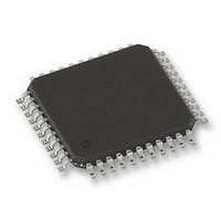
MCU PIC 32KB FLASH 44TQFP
Manufacturer
Microchip Technology
Series
PIC® XLP™ 18Fr
Datasheet
1.PIC18F25K80-ISO.pdf
(628 pages)
Specifications of PIC18F45K80-I/PT
Core Size
8-Bit
Program Memory Size
32KB (16K x 16)
Peripherals
Brown-out Detect/Reset, LVD, POR, PWM, WDT
Core Processor
PIC
Speed
64MHz
Connectivity
ECAN, I²C, LIN, SPI, UART/USART
Number Of I /o
35
Program Memory Type
FLASH
Eeprom Size
1K x 8
Ram Size
3.6K x 8
Voltage - Supply (vcc/vdd)
1.8 V ~ 5.5 V
Data Converters
A/D 11x12b
Oscillator Type
Internal
Operating Temperature
-40°C ~ 85°C
Package / Case
44-TQFP
Controller Family/series
PIC18
Ram Memory Size
4KB
Cpu Speed
16MIPS
No. Of Pwm Channels
5
Embedded Interface Type
I2C, SPI, USART
Processor Series
PIC18F45K80
Core
PIC
Data Bus Width
8 bit
Data Ram Size
1 KB
Interface Type
I2C, SPI, USART
Maximum Clock Frequency
64 MHz
Number Of Programmable I/os
35
Number Of Timers
5
Operating Supply Voltage
1.8 V to 5.5 V
Maximum Operating Temperature
+ 85 C
Mounting Style
SMD/SMT
Lead Free Status / RoHS Status
Lead free / RoHS Compliant
Lead Free Status / RoHS Status
Lead free / RoHS Compliant
Available stocks
Company
Part Number
Manufacturer
Quantity
Price
Company:

Part Number:
PIC18F45K80-I/PT
Manufacturer:
MICROCHIP
Quantity:
1 500
Company:
Part Number:
PIC18F45K80-I/PT
Manufacturer:
PIC
Quantity:
400
Company:
Part Number:
PIC18F45K80-I/PT
Manufacturer:
Microchip Technology
Quantity:
10 000
Part Number:
PIC18F45K80-I/PT
Manufacturer:
MICROCHIP/微芯
Quantity:
20 000


PIC18F66K80 FAMILY
21.3.6
The master can initiate the data transfer at any time
because it controls the SCK. The master determines
when the slave (Processor 1,
broadcast data by the software protocol.
In Master mode, the data is transmitted/received as
soon as the SSPBUF register is written to. If the SPI is
only going to receive, the SDO output could be dis-
abled (programmed as an input). The SSPSR register
will continue to shift in the signal present on the SDI pin
at the programmed clock rate. As each byte is
received, it will be loaded into the SSPBUF register as
if a normal received byte (interrupts and status bits
appropriately set). This could be useful in receiver
applications as a “Line Activity Monitor” mode.
The clock polarity is selected by appropriately
programming the CKP bit (SSPCON1<4>). This then,
would give waveforms for SPI communication as
FIGURE 21-3:
DS39977C-page 298
Write to
SSPBUF
SCK
(CKP = 0
CKE = 0)
SCK
(CKP = 1
CKE = 0)
SCK
(CKP = 0
CKE = 1)
SCK
(CKP = 1
CKE = 1)
SDO
(CKE = 0)
SDO
(CKE = 1)
SDI
(SMP = 0)
Input
Sample
(SMP = 0)
SDI
(SMP = 1)
Input
Sample
(SMP = 1)
SSPIF
SSPSR to
SSPBUF
MASTER MODE
SPI MODE WAVEFORM (MASTER MODE)
bit 7
bit 7
bit 7
bit 7
Figure
bit 6
bit 6
21-2) is to
bit 5
bit 5
Preliminary
bit 4
bit 4
bit 3
bit 3
shown in
where the MSB is transmitted first. In Master mode, the
SPI clock rate (bit rate) is user-programmable to be one
of the following:
• F
• F
• F
• Timer2 output/2
This allows a maximum data rate (at 64 MHz) of
16 Mbps.
Figure 21-3
When the CKE bit is set, the SDO data is valid before
there is a clock edge on SCK. The change of the input
sample is shown based on the state of the SMP bit. The
time when the SSPBUF is loaded with the received
data is shown.
OSC
OSC
OSC
/4 (or T
/16 (or 4 • T
/64 (or 16 • T
bit 2
bit 2
Figure
shows the waveforms for Master mode.
CY
)
bit 1
bit 1
21-3,
CY
CY
)
)
2011 Microchip Technology Inc.
Figure 21-5
bit 0
bit 0
bit 0
bit 0
Next Q4 Cycle
after Q2
and
Four Clock
Modes
Figure
21-6,
Related parts for PIC18F45K80-I/PT
Image
Part Number
Description
Manufacturer
Datasheet
Request
R

Part Number:
Description:
Manufacturer:
Microchip Technology Inc.
Datasheet:
Part Number:
Description:
Manufacturer:
Microchip Technology Inc.
Datasheet:
Part Number:
Description:
Manufacturer:
Microchip Technology Inc.
Datasheet:
Part Number:
Description:
Manufacturer:
Microchip Technology Inc.
Datasheet:
Part Number:
Description:
Manufacturer:
Microchip Technology Inc.
Datasheet:
Part Number:
Description:
Manufacturer:
Microchip Technology Inc.
Datasheet:
Part Number:
Description:
Manufacturer:
Microchip Technology Inc.
Datasheet:
Part Number:
Description:
Manufacturer:
Microchip Technology Inc.
Datasheet: