PIC18F45K80-I/PT Microchip Technology, PIC18F45K80-I/PT Datasheet - Page 307
PIC18F45K80-I/PT
Manufacturer Part Number
PIC18F45K80-I/PT
Description
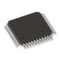
MCU PIC 32KB FLASH 44TQFP
Manufacturer
Microchip Technology
Series
PIC® XLP™ 18Fr
Datasheet
1.PIC18F25K80-ISO.pdf
(628 pages)
Specifications of PIC18F45K80-I/PT
Core Size
8-Bit
Program Memory Size
32KB (16K x 16)
Peripherals
Brown-out Detect/Reset, LVD, POR, PWM, WDT
Core Processor
PIC
Speed
64MHz
Connectivity
ECAN, I²C, LIN, SPI, UART/USART
Number Of I /o
35
Program Memory Type
FLASH
Eeprom Size
1K x 8
Ram Size
3.6K x 8
Voltage - Supply (vcc/vdd)
1.8 V ~ 5.5 V
Data Converters
A/D 11x12b
Oscillator Type
Internal
Operating Temperature
-40°C ~ 85°C
Package / Case
44-TQFP
Controller Family/series
PIC18
Ram Memory Size
4KB
Cpu Speed
16MIPS
No. Of Pwm Channels
5
Embedded Interface Type
I2C, SPI, USART
Processor Series
PIC18F45K80
Core
PIC
Data Bus Width
8 bit
Data Ram Size
1 KB
Interface Type
I2C, SPI, USART
Maximum Clock Frequency
64 MHz
Number Of Programmable I/os
35
Number Of Timers
5
Operating Supply Voltage
1.8 V to 5.5 V
Maximum Operating Temperature
+ 85 C
Mounting Style
SMD/SMT
Lead Free Status / RoHS Status
Lead free / RoHS Compliant
Lead Free Status / RoHS Status
Lead free / RoHS Compliant
Available stocks
Company
Part Number
Manufacturer
Quantity
Price
Company:

Part Number:
PIC18F45K80-I/PT
Manufacturer:
MICROCHIP
Quantity:
1 500
Company:
Part Number:
PIC18F45K80-I/PT
Manufacturer:
PIC
Quantity:
400
Company:
Part Number:
PIC18F45K80-I/PT
Manufacturer:
Microchip Technology
Quantity:
10 000
Part Number:
PIC18F45K80-I/PT
Manufacturer:
MICROCHIP/微芯
Quantity:
20 000


21.4.2
The MSSP module functions are enabled by setting the
MSSP Enable bit, SSPEN (SSPCON1<5>).
The SSPCON1 register allows control of the I
operation. Four mode selection bits (SSPCON1<3:0>)
allow one of the following I
• I
• I
• I
• I
• I
• I
Selection of any I
forces the SCL and SDA pins to be open-drain,
provided these pins are programmed as inputs by
setting the appropriate TRISC bit. To ensure proper
operation of the module, pull-up resistors must be
provided externally to the SCL and SDA pins.
21.4.3
In Slave mode, the SCL and SDA pins must be
configured as inputs (TRISC<4:3> set). The MSSP
module will override the input state with the output data
when required (slave-transmitter).
The I
interrupt on an address match. Address masking will
allow the hardware to generate an interrupt for more
than one address (up to 31 in 7-bit addressing and up
to 63 in 10-bit addressing). Through the mode select
bits, the user can also choose to interrupt on Start and
Stop bits.
When an address is matched, or the data transfer after
an address match is received, the hardware auto-
matically will generate the Acknowledge (ACK) pulse
and load the SSPBUF register with the received value
currently in the SSPSR register.
Any combination of the following conditions will cause
the MSSP module not to give this ACK pulse:
• The Buffer Full bit, BF (SSPSTAT<0>), was set
• The overflow bit, SSPOV (SSPCON1<6>), was
In this case, the SSPSR register value is not loaded
into the SSPBUF, but bit, SSPIF, is set. The BF bit is
cleared by reading the SSPBUF register, while bit,
SSPOV, is cleared through software.
The SCL clock input must have a minimum high and
low for proper operation. The high and low times of the
I
MSSP module, are shown in timing Parameter 100 and
Parameter 101.
2011 Microchip Technology Inc.
2
C specification, as well as the requirement of the
Stop bit interrupts enabled
Stop bit interrupts enabled
Idle
before the transfer was received.
set before the transfer was received.
2
2
2
2
2
2
C Master mode, clock
C Slave mode (7-bit address)
C Slave mode (10-bit address)
C Slave mode (7-bit address) with Start and
C Slave mode (10-bit address) with Start and
C Firmware Controlled Master mode, slave is
2
C Slave mode hardware will always generate an
OPERATION
SLAVE MODE
2
C mode with the SSPEN bit set
2
C modes to be selected:
Preliminary
2
C
PIC18F66K80 FAMILY
21.4.3.1
Once the MSSP module has been enabled, it waits for
a Start condition to occur. Following the Start condition,
the 8 bits are shifted into the SSPSR register. All incom-
ing bits are sampled with the rising edge of the clock
(SCL) line. The value of register, SSPSR<7:1>, is com-
pared to the value of the SSPADD register. The
address is compared on the falling edge of the eighth
clock (SCL) pulse. If the addresses match and the BF
and SSPOV bits are clear, the following events occur:
1.
2.
3.
4.
In 10-Bit Addressing mode, two address bytes need to
be received by the slave. The five Most Significant bits
(MSbs) of the first address byte specify if this is a 10-bit
address. The R/W (SSPSTAT<2>) bit must specify a
write so the slave device will receive the second
address byte. For a 10-bit address, the first byte would
equal ‘ 11110 A9 A8 0 ’, where ‘ A9 ’ and ‘ A8 ’ are the
two MSbs of the address. The sequence of events for
10-bit addressing is as follows, with steps, 7 through 9,
for the slave-transmitter:
1.
2.
3.
4.
5.
6.
7.
8.
9.
The SSPSR register value is loaded into the
SSPBUF register.
The Buffer Full bit, BF, is set.
An ACK pulse is generated.
The MSSP Interrupt Flag bit, SSPIF, is set (and
interrupt is generated, if enabled) on the falling
edge of the ninth SCL pulse.
Receive first (high) byte of address (bits, SSPIF,
BF and UA, are set on address match).
Update the SSPADD register with second (low)
byte of address (clears bit, UA, and releases the
SCL line).
Read the SSPBUF register (clears bit, BF) and
clear flag bit, SSPIF.
Receive second (low) byte of address (bits,
SSPIF, BF and UA, are set).
Update the SSPADD register with the first (high)
byte of address. If match releases SCL line, this
will clear bit, UA.
Read the SSPBUF register (clears bit, BF) and
clear flag bit SSPIF.
Receive Repeated Start condition.
Receive first (high) byte of address (bits, SSPIF
and BF, are set).
Read the SSPBUF register (clears bit, BF) and
clear flag bit, SSPIF.
Addressing
DS39977C-page 307
Related parts for PIC18F45K80-I/PT
Image
Part Number
Description
Manufacturer
Datasheet
Request
R

Part Number:
Description:
Manufacturer:
Microchip Technology Inc.
Datasheet:
Part Number:
Description:
Manufacturer:
Microchip Technology Inc.
Datasheet:
Part Number:
Description:
Manufacturer:
Microchip Technology Inc.
Datasheet:
Part Number:
Description:
Manufacturer:
Microchip Technology Inc.
Datasheet:
Part Number:
Description:
Manufacturer:
Microchip Technology Inc.
Datasheet:
Part Number:
Description:
Manufacturer:
Microchip Technology Inc.
Datasheet:
Part Number:
Description:
Manufacturer:
Microchip Technology Inc.
Datasheet:
Part Number:
Description:
Manufacturer:
Microchip Technology Inc.
Datasheet: