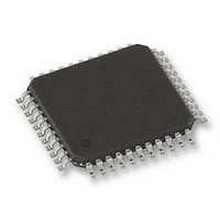
PIC18F45K80-I/PT Microchip Technology, PIC18F45K80-I/PT Datasheet - Page 381

PIC18F45K80-I/PT
Manufacturer Part Number
PIC18F45K80-I/PT
Description
MCU PIC 32KB FLASH 44TQFP
Manufacturer
Microchip Technology
Series
PIC® XLP™ 18Fr
Datasheet
1.PIC18F25K80-ISO.pdf
(628 pages)
Specifications of PIC18F45K80-I/PT
Core Size
8-Bit
Program Memory Size
32KB (16K x 16)
Peripherals
Brown-out Detect/Reset, LVD, POR, PWM, WDT
Core Processor
PIC
Speed
64MHz
Connectivity
ECAN, I²C, LIN, SPI, UART/USART
Number Of I /o
35
Program Memory Type
FLASH
Eeprom Size
1K x 8
Ram Size
3.6K x 8
Voltage - Supply (vcc/vdd)
1.8 V ~ 5.5 V
Data Converters
A/D 11x12b
Oscillator Type
Internal
Operating Temperature
-40°C ~ 85°C
Package / Case
44-TQFP
Controller Family/series
PIC18
Ram Memory Size
4KB
Cpu Speed
16MIPS
No. Of Pwm Channels
5
Embedded Interface Type
I2C, SPI, USART
Processor Series
PIC18F45K80
Core
PIC
Data Bus Width
8 bit
Data Ram Size
1 KB
Interface Type
I2C, SPI, USART
Maximum Clock Frequency
64 MHz
Number Of Programmable I/os
35
Number Of Timers
5
Operating Supply Voltage
1.8 V to 5.5 V
Maximum Operating Temperature
+ 85 C
Mounting Style
SMD/SMT
Lead Free Status / RoHS Status
Lead free / RoHS Compliant
Lead Free Status / RoHS Status
Lead free / RoHS Compliant
Available stocks
Company
Part Number
Manufacturer
Quantity
Price
Company:
Part Number:
PIC18F45K80-I/PT
Manufacturer:
MICROCHIP
Quantity:
1 500
Company:
Part Number:
PIC18F45K80-I/PT
Manufacturer:
PIC
Quantity:
400
Company:
Part Number:
PIC18F45K80-I/PT
Manufacturer:
Microchip Technology
Quantity:
10 000
Part Number:
PIC18F45K80-I/PT
Manufacturer:
MICROCHIP/微芯
Quantity:
20 000
- Current page: 381 of 628
- Download datasheet (6Mb)
24.5
Each comparator has up to eight possible combina-
tions of inputs: up to four external analog inputs and
one of two internal voltage references.
All of the comparators allow a selection of the signal
from pin, CxINA, or the voltage from the comparator
reference (CV
compared to either C1INB, CxINC, C2INB or the micro-
controller’s fixed internal reference voltage (V
1.024V nominal) on the inverting channel. The compar-
ator inputs and outputs are tied to fixed I/O pins,
defined in
urations and their corresponding bit settings are shown
in
TABLE 24-1:
24.5.1
Setting the CON bit of the CMxCON register
(CMxCON<7>) enables the comparator for operation.
Clearing the CON bit disables the comparator, resulting
in minimum current consumption.
The CCH<1:0> bits in the CMxCON register
(CMxCON<1:0>) direct either one of three analog input
pins, or the Internal Reference Voltage (V
comparator, V
ating mode, either an external or internal voltage
reference may be used.
The analog signal present at V
signal at V
is adjusted accordingly.
2011 Microchip Technology Inc.
Comparator
Figure
† The I/O pin is dependent on package type.
1
2
Comparator Control and
Configuration
24-4.
Table
IN
COMPARATOR ENABLE AND
INPUT SELECTION
+ and the digital output of the comparator
REF
IN
-. Depending on the comparator oper-
24-1. The available comparator config-
) on the non-inverting channel. This is
COMPARATOR INPUTS AND
OUTPUTS
Input or Output
C1INA (V
C1INB (V
C1INC (V
C2INA(V
C2INB(V
C2INB(V
C2INC(V
C1OUT
C2OUT
IN
IN
IN
IN
IN
IN
IN
IN
+)
+)
-)
-)
-)
-)
-)
- is compared to the
RB0/RD0
RB1/RD1
RA5/RD3
RA5/RD3
I/O Pin
RB2/RE1
RB4/RD2
RB3/RE2
BG
RA1
RA2
), to the
(†)
Preliminary
BG
,
PIC18F66K80 FAMILY
The external reference is used when CREF = 0
(CMxCON<2>) and V
pin. When external voltage references are used, the
comparator module can be configured to have the ref-
erence sources externally. The reference signal must
be between V
pin of the comparator.
The comparator module also allows the selection of an
internally generated voltage reference (CV
comparator voltage reference module. This module is
described in more detail in
Voltage Reference Module”
comparator voltage reference module is only available
when CREF = 1 . In this mode, the internal voltage
reference is applied to the comparator’s V
24.5.2
The comparator outputs are read through the CMSTAT
register. The CMSTAT<6> bit reads the Comparator 1
output, CMSTAT<7> reads the Comparator 2 output.
These bits are read-only.
The comparator outputs may also be directly output to
the RE2 and RE1 pins by setting the COE bit
(CMxCON<6>). When enabled, multiplexers in the
output path of the pins switch to the output of the com-
parator. While in this mode, the TRISE<2:1> bits still
function as the digital output enable bits for the RE2,
and RE1 pins.
By default, the comparator’s output is at logic high
whenever the voltage on V
The polarity of the comparator outputs can be inverted
using the CPOL bit (CMxCON<5>).
The uncertainty of each of the comparators is related to
the input offset voltage and the response time given in
the specifications, as discussed in
“Comparator Operation”
Note:
The comparator input pin selected by
CCH<1:0> must be configured as an input
by setting both the corresponding TRIS bit
and the corresponding ANSELx bit in the
ANCONx register.
COMPARATOR ENABLE AND
OUTPUT SELECTION
SS
and V
IN
DD
+ is connected to the CxINA
and can be applied to either
.
Section 25.0 “Comparator
IN
+ is greater than on V
. The reference from the
DS39977C-page 381
IN
Section 24.2
REF
+ pin.
) from the
IN
-.
Related parts for PIC18F45K80-I/PT
Image
Part Number
Description
Manufacturer
Datasheet
Request
R

Part Number:
Description:
Manufacturer:
Microchip Technology Inc.
Datasheet:

Part Number:
Description:
Manufacturer:
Microchip Technology Inc.
Datasheet:

Part Number:
Description:
Manufacturer:
Microchip Technology Inc.
Datasheet:

Part Number:
Description:
Manufacturer:
Microchip Technology Inc.
Datasheet:

Part Number:
Description:
Manufacturer:
Microchip Technology Inc.
Datasheet:

Part Number:
Description:
Manufacturer:
Microchip Technology Inc.
Datasheet:

Part Number:
Description:
Manufacturer:
Microchip Technology Inc.
Datasheet:

Part Number:
Description:
Manufacturer:
Microchip Technology Inc.
Datasheet:


