PIC18F45K80-I/PT Microchip Technology, PIC18F45K80-I/PT Datasheet - Page 442
PIC18F45K80-I/PT
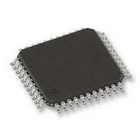
Manufacturer Part Number
PIC18F45K80-I/PT
Description
MCU PIC 32KB FLASH 44TQFP
Manufacturer
Microchip Technology
Series
PIC® XLP™ 18Fr
Datasheet
1.PIC18F25K80-ISO.pdf
(628 pages)
Specifications of PIC18F45K80-I/PT
Core Size
8-Bit
Program Memory Size
32KB (16K x 16)
Peripherals
Brown-out Detect/Reset, LVD, POR, PWM, WDT
Core Processor
PIC
Speed
64MHz
Connectivity
ECAN, I²C, LIN, SPI, UART/USART
Number Of I /o
35
Program Memory Type
FLASH
Eeprom Size
1K x 8
Ram Size
3.6K x 8
Voltage - Supply (vcc/vdd)
1.8 V ~ 5.5 V
Data Converters
A/D 11x12b
Oscillator Type
Internal
Operating Temperature
-40°C ~ 85°C
Package / Case
44-TQFP
Controller Family/series
PIC18
Ram Memory Size
4KB
Cpu Speed
16MIPS
No. Of Pwm Channels
5
Embedded Interface Type
I2C, SPI, USART
Processor Series
PIC18F45K80
Core
PIC
Data Bus Width
8 bit
Data Ram Size
1 KB
Interface Type
I2C, SPI, USART
Maximum Clock Frequency
64 MHz
Number Of Programmable I/os
35
Number Of Timers
5
Operating Supply Voltage
1.8 V to 5.5 V
Maximum Operating Temperature
+ 85 C
Mounting Style
SMD/SMT
Lead Free Status / RoHS Status
Lead free / RoHS Compliant
Lead Free Status / RoHS Status
Lead free / RoHS Compliant
Available stocks
Company
Part Number
Manufacturer
Quantity
Price
Company:

Part Number:
PIC18F45K80-I/PT
Manufacturer:
MICROCHIP
Quantity:
1 500
Company:
Part Number:
PIC18F45K80-I/PT
Manufacturer:
PIC
Quantity:
400
Company:
Part Number:
PIC18F45K80-I/PT
Manufacturer:
Microchip Technology
Quantity:
10 000
Part Number:
PIC18F45K80-I/PT
Manufacturer:
MICROCHIP/微芯
Quantity:
20 000


PIC18F66K80 FAMILY
27.3
The PIC18F66K80 family has six main modes of
operation:
• Configuration mode
• Disable/Sleep mode
• Normal Operation mode
• Listen Only mode
• Loopback mode
• Error Recognition mode
All modes, except Error Recognition, are requested by
setting the REQOP bits (CANCON<7:5>). Error Recog-
nition mode is requested through the RXM bits of the
Receive Buffer register(s). Entry into a mode is
Acknowledged by monitoring the OPMODE bits.
When changing modes, the mode will not actually
change until all pending message transmissions are
complete. Because of this, the user must verify that the
device has actually changed into the requested mode
before further operations are executed.
27.3.1
The CAN module has to be initialized before the
activation. This is only possible if the module is in the
Configuration mode. The Configuration mode is
requested by setting the REQOP2 bit. Only when the
status bit, OPMODE2, has a high level can the initial-
ization be performed. Afterwards, the Configuration
registers, the acceptance mask registers and the
acceptance filter registers can be written. The module
is activated by setting the REQOP control bits to zero.
The module will protect the user from accidentally
violating the CAN protocol through programming
errors. All registers which control the configuration of
the module can not be modified while the module is on-
line. The CAN module will not be allowed to enter the
Configuration mode while a transmission or reception
is taking place. The Configuration mode serves as a
lock to protect the following registers:
• Configuration Registers
• Functional Mode Selection Registers
• Bit Timing Registers
• Identifier Acceptance Filter Registers
• Identifier Acceptance Mask Registers
• Filter and Mask Control Registers
• Mask Selection Registers
In the Configuration mode, the module will not transmit
or receive. The error counters are cleared and the inter-
rupt flags remain unchanged. The programmer will
have access to Configuration registers that are access
restricted in other modes. I/O pins will revert to normal
I/O functions
DS39977C-page 442
CAN Modes of Operation
CONFIGURATION MODE
.
Preliminary
27.3.2
In Disable/Sleep mode, the module will not transmit or
receive. The module has the ability to set the WAKIF bit
due to bus activity; however, any pending interrupts will
remain and the error counters will retain their value.
If the REQOP<2:0> bits are set to ‘ 001 ’, the module will
enter the module Disable/Sleep mode. This mode is
similar to disabling other peripheral modules by turning
off the module enables. This causes the module
internal clock to stop unless the module is active (i.e.,
receiving or transmitting a message). If the module is
active, the module will wait for 11 recessive bits on the
CAN bus, detect that condition as an Idle bus, then
accept
OPMODE<2:0> = 001 indicates whether the module
successfully went into the module Disable/Sleep mode.
The WAKIF interrupt is the only module interrupt that is
still active in the Disable/Sleep mode. If the WAKDIS is
cleared and WAKIE is set, the processor will receive an
interrupt whenever the module detects recessive to
dominant transition. On wake-up, the module will auto-
matically be set to the previous mode of operation. For
example, if the module was switched from Normal to
Disable/Sleep mode on bus activity wake-up, the
module will automatically enter into Normal mode and
the first message that caused the module to wake-up is
lost. The module will not generate any error frame.
Firmware logic must detect this condition and make
sure that retransmission is requested. If the processor
receives a wake-up interrupt while it is sleeping, more
than one message may get lost. The actual number of
messages lost would depend on the processor
oscillator start-up time and incoming message bit rate.
The TXCAN pin will stay in the recessive state while the
module is in Disable/Sleep mode.
27.3.3
This is the standard operating mode of the
PIC18F66K80 family devices. In this mode, the device
actively monitors all bus messages and generates
Acknowledge bits, error frames, etc. This is also the
only mode in which the PIC18F66K80 family devices
will transmit messages over the CAN bus.
the
DISABLE/SLEEP MODE
NORMAL MODE
module
2011 Microchip Technology Inc.
Disable/Sleep
command.
Related parts for PIC18F45K80-I/PT
Image
Part Number
Description
Manufacturer
Datasheet
Request
R

Part Number:
Description:
Manufacturer:
Microchip Technology Inc.
Datasheet:
Part Number:
Description:
Manufacturer:
Microchip Technology Inc.
Datasheet:
Part Number:
Description:
Manufacturer:
Microchip Technology Inc.
Datasheet:
Part Number:
Description:
Manufacturer:
Microchip Technology Inc.
Datasheet:
Part Number:
Description:
Manufacturer:
Microchip Technology Inc.
Datasheet:
Part Number:
Description:
Manufacturer:
Microchip Technology Inc.
Datasheet:
Part Number:
Description:
Manufacturer:
Microchip Technology Inc.
Datasheet:
Part Number:
Description:
Manufacturer:
Microchip Technology Inc.
Datasheet: