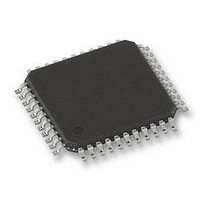
PIC18F45K80-I/PT Microchip Technology, PIC18F45K80-I/PT Datasheet - Page 503

PIC18F45K80-I/PT
Manufacturer Part Number
PIC18F45K80-I/PT
Description
MCU PIC 32KB FLASH 44TQFP
Manufacturer
Microchip Technology
Series
PIC® XLP™ 18Fr
Datasheet
1.PIC18F25K80-ISO.pdf
(628 pages)
Specifications of PIC18F45K80-I/PT
Core Size
8-Bit
Program Memory Size
32KB (16K x 16)
Peripherals
Brown-out Detect/Reset, LVD, POR, PWM, WDT
Core Processor
PIC
Speed
64MHz
Connectivity
ECAN, I²C, LIN, SPI, UART/USART
Number Of I /o
35
Program Memory Type
FLASH
Eeprom Size
1K x 8
Ram Size
3.6K x 8
Voltage - Supply (vcc/vdd)
1.8 V ~ 5.5 V
Data Converters
A/D 11x12b
Oscillator Type
Internal
Operating Temperature
-40°C ~ 85°C
Package / Case
44-TQFP
Controller Family/series
PIC18
Ram Memory Size
4KB
Cpu Speed
16MIPS
No. Of Pwm Channels
5
Embedded Interface Type
I2C, SPI, USART
Processor Series
PIC18F45K80
Core
PIC
Data Bus Width
8 bit
Data Ram Size
1 KB
Interface Type
I2C, SPI, USART
Maximum Clock Frequency
64 MHz
Number Of Programmable I/os
35
Number Of Timers
5
Operating Supply Voltage
1.8 V to 5.5 V
Maximum Operating Temperature
+ 85 C
Mounting Style
SMD/SMT
Lead Free Status / RoHS Status
Lead free / RoHS Compliant
Lead Free Status / RoHS Status
Lead free / RoHS Compliant
Available stocks
Company
Part Number
Manufacturer
Quantity
Price
Company:
Part Number:
PIC18F45K80-I/PT
Manufacturer:
MICROCHIP
Quantity:
1 500
Company:
Part Number:
PIC18F45K80-I/PT
Manufacturer:
PIC
Quantity:
400
Company:
Part Number:
PIC18F45K80-I/PT
Manufacturer:
Microchip Technology
Quantity:
10 000
Part Number:
PIC18F45K80-I/PT
Manufacturer:
MICROCHIP/微芯
Quantity:
20 000
- Current page: 503 of 628
- Download datasheet (6Mb)
CLRF
Syntax:
Operands:
Operation:
Status Affected:
Encoding:
Description:
Words:
Cycles:
Example:
2011 Microchip Technology Inc.
Q Cycle Activity:
Before Instruction
After Instruction
Decode
FLAG_REG
FLAG_REG
Q1
register ‘f’
Clear f
CLRF
0 f 255
a [0,1]
000h f,
1 Z
Z
Clears the contents of the specified
register.
If ‘a’ is ‘ 0 ’, the Access Bank is selected.
If ‘a’ is ‘ 1 ’, the BSR is used to select the
GPR bank.
If ‘a’ is ‘ 0 ’ and the extended instruction
set is enabled, this instruction operates
in Indexed Literal Offset Addressing
mode whenever f 95 (5Fh). See
Section 29.2.3 “Byte-Oriented and
Bit-Oriented Instructions in Indexed
Literal Offset Mode”
1
1
CLRF
Read
0110
Q2
=
=
f {,a}
5Ah
00h
101a
FLAG_REG,1
Process
Data
Q3
ffff
for details.
register ‘f’
Write
Q4
ffff
Preliminary
PIC18F66K80 FAMILY
CLRWDT
Syntax:
Operands:
Operation:
Status Affected:
Encoding:
Description:
Words:
Cycles:
Example:
Q Cycle Activity:
Before Instruction
After Instruction
Decode
WDT Counter
WDT Counter
WDT Postscaler
TO
PD
Q1
operation
Clear Watchdog Timer
CLRWDT
None
000h WDT,
000h WDT postscaler,
1 TO,
1 PD
TO, PD
CLRWDT instruction resets the
Watchdog Timer. It also resets the
postscaler of the WDT. Status bits, TO
and PD, are set.
1
1
CLRWDT
0000
No
Q2
=
=
=
=
=
0000
?
00h
0
1
1
Process
Data
Q3
DS39977C-page 503
0000
operation
No
Q4
0100
Related parts for PIC18F45K80-I/PT
Image
Part Number
Description
Manufacturer
Datasheet
Request
R

Part Number:
Description:
Manufacturer:
Microchip Technology Inc.
Datasheet:

Part Number:
Description:
Manufacturer:
Microchip Technology Inc.
Datasheet:

Part Number:
Description:
Manufacturer:
Microchip Technology Inc.
Datasheet:

Part Number:
Description:
Manufacturer:
Microchip Technology Inc.
Datasheet:

Part Number:
Description:
Manufacturer:
Microchip Technology Inc.
Datasheet:

Part Number:
Description:
Manufacturer:
Microchip Technology Inc.
Datasheet:

Part Number:
Description:
Manufacturer:
Microchip Technology Inc.
Datasheet:

Part Number:
Description:
Manufacturer:
Microchip Technology Inc.
Datasheet:


