PIC18F45K80-I/PT Microchip Technology, PIC18F45K80-I/PT Datasheet - Page 615
PIC18F45K80-I/PT
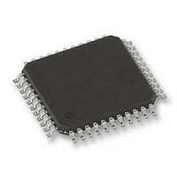
Manufacturer Part Number
PIC18F45K80-I/PT
Description
MCU PIC 32KB FLASH 44TQFP
Manufacturer
Microchip Technology
Series
PIC® XLP™ 18Fr
Datasheet
1.PIC18F25K80-ISO.pdf
(628 pages)
Specifications of PIC18F45K80-I/PT
Core Size
8-Bit
Program Memory Size
32KB (16K x 16)
Peripherals
Brown-out Detect/Reset, LVD, POR, PWM, WDT
Core Processor
PIC
Speed
64MHz
Connectivity
ECAN, I²C, LIN, SPI, UART/USART
Number Of I /o
35
Program Memory Type
FLASH
Eeprom Size
1K x 8
Ram Size
3.6K x 8
Voltage - Supply (vcc/vdd)
1.8 V ~ 5.5 V
Data Converters
A/D 11x12b
Oscillator Type
Internal
Operating Temperature
-40°C ~ 85°C
Package / Case
44-TQFP
Controller Family/series
PIC18
Ram Memory Size
4KB
Cpu Speed
16MIPS
No. Of Pwm Channels
5
Embedded Interface Type
I2C, SPI, USART
Processor Series
PIC18F45K80
Core
PIC
Data Bus Width
8 bit
Data Ram Size
1 KB
Interface Type
I2C, SPI, USART
Maximum Clock Frequency
64 MHz
Number Of Programmable I/os
35
Number Of Timers
5
Operating Supply Voltage
1.8 V to 5.5 V
Maximum Operating Temperature
+ 85 C
Mounting Style
SMD/SMT
Lead Free Status / RoHS Status
Lead free / RoHS Compliant
Lead Free Status / RoHS Status
Lead free / RoHS Compliant
Available stocks
Company
Part Number
Manufacturer
Quantity
Price
Company:

Part Number:
PIC18F45K80-I/PT
Manufacturer:
MICROCHIP
Quantity:
1 500
Company:
Part Number:
PIC18F45K80-I/PT
Manufacturer:
PIC
Quantity:
400
Company:
Part Number:
PIC18F45K80-I/PT
Manufacturer:
Microchip Technology
Quantity:
10 000
Part Number:
PIC18F45K80-I/PT
Manufacturer:
MICROCHIP/微芯
Quantity:
20 000


F
Fail-Safe Clock Monitor............................................. 461, 481
Fast Register Stack........................................................... 109
Firmware Instructions........................................................ 487
Flash Program Memory .................................................... 135
FSCM. See Fail-Safe Clock Monitor.
G
GOTO ............................................................................... 508
H
Hardware Multiplier ........................................................... 151
High/Low-Voltage Detect .................................................. 389
HLVD. See High/Low-Voltage Detect. .............................. 389
I
I/O Descriptions
I/O Ports ............................................................................ 177
I
2011 Microchip Technology Inc.
2
C Mode (MSSP)
Exiting Operation ...................................................... 481
Interrupts in Power-Managed Modes........................ 482
POR or Wake from Sleep ......................................... 482
WDT During Oscillator Failure .................................. 481
Associated Registers ................................................ 143
Control Registers ...................................................... 136
Erase Sequence ....................................................... 140
Erasing...................................................................... 140
Operation During Code-Protect ................................ 143
Reading..................................................................... 139
Table Pointer
Table Pointer Boundaries ......................................... 138
Table Reads and Table Writes ................................. 135
Write Sequence ........................................................ 141
Writing....................................................................... 141
8 x 8 Multiplication Algorithms .................................. 151
Operation .................................................................. 151
Performance Comparison (table).............................. 151
Applications............................................................... 393
Associated Registers ................................................ 394
Current Consumption................................................ 391
Effects of a Reset...................................................... 394
Operation .................................................................. 390
Setup......................................................................... 391
Start-up Time ............................................................ 391
Typical Application .................................................... 393
PIC18F2XK80 ............................................................. 20
PIC18F4XK80 ............................................................. 26
PIC18F6XK80 ............................................................. 35
Analog, Digital Ports ................................................. 180
Open-Drain Outputs.................................................. 179
Output Pin Drive........................................................ 177
Pin Capabilities ......................................................... 177
Port Slew Rate .......................................................... 180
Pull-up Configuration ................................................ 177
Acknowledge Sequence Timing................................ 331
Associated Registers ................................................ 337
Baud Rate Generator................................................ 324
EECON1 and EECON2 .................................... 136
TABLAT (Table Latch) Register........................ 138
TBLPTR (Table Pointer) Register ..................... 138
Boundaries Based on Operation....................... 138
Protection Against Spurious Writes .................. 143
Unexpected Termination................................... 143
Write Verify ....................................................... 143
During Sleep ..................................................... 394
Preliminary
PIC18F66K80 FAMILY
ID Locations.............................................................. 461, 486
Idle Modes .......................................................................... 72
INCF ................................................................................. 508
INCFSZ............................................................................. 509
In-Circuit Debugger........................................................... 486
In-Circuit Serial Programming (ICSP)....................... 461, 486
Indexed Literal Offset Addressing
Indexed Literal Offset Mode.............................................. 534
Indirect Addressing ........................................................... 129
INFSNZ............................................................................. 509
Initialization Conditions for all Registers ............................. 90
Instruction Cycle ............................................................... 110
Instruction Set................................................................... 487
Bus Collision
Clock Arbitration ....................................................... 325
Clock Stretching ....................................................... 317
Clock Synchronization and the CKP bit.................... 318
Effects of a Reset ..................................................... 332
General Call Address Support.................................. 321
I
Master Mode............................................................. 322
Multi-Master Communication, Bus Collision
Multi-Master Mode.................................................... 332
Operation.................................................................. 307
Read/Write Bit Information (R/W Bit)................ 307, 310
Registers .................................................................. 302
Serial Clock (RC3REFO//SCL/SCK) ........................ 310
Slave Mode............................................................... 307
Sleep Operation........................................................ 332
Stop Condition Timing .............................................. 331
and Standard PIC18 Instructions.............................. 534
Clocking Scheme...................................................... 110
Flow/Pipelining ......................................................... 110
ADDLW..................................................................... 493
ADDWF .................................................................... 493
ADDWF (Indexed Literal Offset Mode) ..................... 535
ADDWFC.................................................................. 494
ANDLW..................................................................... 494
ANDWF .................................................................... 495
BC............................................................................. 495
BCF .......................................................................... 496
BN............................................................................. 496
BNC .......................................................................... 497
BNN .......................................................................... 497
BNOV ....................................................................... 498
BNZ .......................................................................... 498
BOV .......................................................................... 501
2
C Clock Rate w/BRG ............................................. 324
During a Repeated Start Condition................... 335
During a Stop Condition ................................... 336
10-Bit Slave Receive Mode (SEN = 1) ............. 317
10-Bit Slave Transmit Mode ............................. 317
7-Bit Slave Receive Mode (SEN = 1) ............... 317
7-Bit Slave Transmit Mode ............................... 317
Operation.......................................................... 323
Reception ......................................................... 328
Repeated Start Condition Timing ..................... 327
Start Condition Timing ...................................... 326
Transmission .................................................... 328
and Arbitration .................................................. 332
Address Masking Modes
Addressing ....................................................... 307
Reception ......................................................... 310
Transmission .................................................... 310
5-Bit .......................................................... 308
7-Bit .......................................................... 309
DS39977C-page 615
Related parts for PIC18F45K80-I/PT
Image
Part Number
Description
Manufacturer
Datasheet
Request
R

Part Number:
Description:
Manufacturer:
Microchip Technology Inc.
Datasheet:
Part Number:
Description:
Manufacturer:
Microchip Technology Inc.
Datasheet:
Part Number:
Description:
Manufacturer:
Microchip Technology Inc.
Datasheet:
Part Number:
Description:
Manufacturer:
Microchip Technology Inc.
Datasheet:
Part Number:
Description:
Manufacturer:
Microchip Technology Inc.
Datasheet:
Part Number:
Description:
Manufacturer:
Microchip Technology Inc.
Datasheet:
Part Number:
Description:
Manufacturer:
Microchip Technology Inc.
Datasheet:
Part Number:
Description:
Manufacturer:
Microchip Technology Inc.
Datasheet: