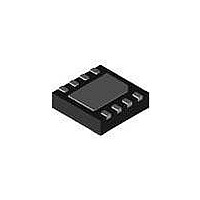
NCP5901MNTBG ON Semiconductor, NCP5901MNTBG Datasheet - Page 4

NCP5901MNTBG
Manufacturer Part Number
NCP5901MNTBG
Description
IC MOSFET DVR SYNC VR12 8-DFN
Manufacturer
ON Semiconductor
Type
VR12 Compatible Synchronous Buck MOSFET Driverr
Datasheet
1.NCP5901DR2G.pdf
(9 pages)
Specifications of NCP5901MNTBG
Configuration
High and Low Side, Synchronous
Input Type
Non-Inverting
Delay Time
25ns
Number Of Configurations
1
Number Of Outputs
2
Mounting Type
Surface Mount
Package / Case
8-DFN
Product
MOSFET Gate Drivers
Propagation Delay Time
25 ns
Mounting Style
SMD/SMT
Number Of Drivers
1
Output Voltage
35 V
Lead Free Status / RoHS Status
Lead free / RoHS Compliant
Current - Peak
-
High Side Voltage - Max (bootstrap)
-
Voltage - Supply
-
Operating Temperature
-
Lead Free Status / Rohs Status
Lead free / RoHS Compliant
Available stocks
Company
Part Number
Manufacturer
Quantity
Price
Company:
Part Number:
NCP5901MNTBG
Manufacturer:
ON Semiconductor
Quantity:
1 400
Part Number:
NCP5901MNTBG
Manufacturer:
ON/安森美
Quantity:
20 000
Table 4. ELECTRICAL CHARACTERISTICS
4.5 V < BST−SWN < 13.2 V, 4.5 V < BST < 30 V, 0 V < SWN < 21 V)
SUPPLY VOLTAGE
UNDERVOLTAGE LOCKOUT
SUPPLY CURRENT
PWM INPUT
HIGH SIDE DRIVER (VCC = 12 V)
HIGH SIDE DRIVER (VCC = 5 V)
VCC Operation Voltage
Power ON Reset Threshold
VCC Start Threshold
VCC UVLO Hysteresis
Output Overvoltage Trip Threshold at
Startup
Normal Mode
Standby Current
Standby Current
Standby Current
PWM Input High
PWM Mid−State
PWM Input Low
ZCD Blanking Timer
Output Impedance, Sourcing Current
Output Impedance, Sinking Current
DRVH Rise Time tr
DRVH Fall Time tf
DRVH Turn−Off Propagation Delay
tpdh
DRVH Turn−On Propagation Delay
tpdl
SW Pull Down Resistance
DRVH Pull Down Resistance
Output Impedance, Sourcing Current
Output Impedance, Sinking Current
DRVH Rise Time tr
DRVH Fall Time tf
DRVH Turn−Off Propagation Delay
tpdh
DRVH Turn−On Propagation Delay
tpdl
SW Pull Down Resistance
DRVH Pull Down Resistance
DRVH
DRVH
DRVH
DRVH
Parameter
DRVH
DRVH
DRVH
DRVH
Power Startup time, VCC > POR
Icc + Ibst, EN = 5 V, PWM = OSC, Fsw = 100 KHz,
Cload = 3 nF for DRVH, 3 nF for DRVL
Icc + Ibst, EN = GND
I
No loading on DRVH & DRVL
I
No loading on DRVH & DRVL
VBST − VSW = 12 V
VBST − VSW = 12 V
V
V
C
C
SW to PGND
DRVH to SW, BST−SW = 0 V
VBST − VSW = 5 V
VBST − VSW = 5 V
V
V
C
C
SW to PGND
DRVH to SW, BST−SW = 0 V
CC
CC
VCC
VCC
LOAD
LOAD
VCC
VCC
LOAD
LOAD
+ I
+ I
= 12 V, 3 nF load, VBST−VSW = 12 V
= 12 V, 3 nF load, VBST−VSW = 12 V
= 5 V, 3 nF load, VBST − VSW = 5 V
= 5 V, 3 nF load, VBST − VSW = 5 V
BST
BST
(
= 3 nF
= 3 nF
= 3 nF
= 3 nF
Unless otherwise stated: −10°C < T
, EN = HIGH, PWM = LOW,
, EN = HIGH, PWM = HIGH,
http://onsemi.com
Test Conditions
4
A
< +125°C; 4.5 V < V
Min.
150
4.5
3.8
2.1
3.4
1.3
8.0
CC
Typ.
2.75
4.35
2.25
12.2
200
250
0.5
2.1
2.2
2.0
1.0
4.5
2.9
< 13.2 V,
16
11
45
45
30
27
20
27
45
45
Max.
13.2
250
3.2
4.5
2.4
1.9
2.7
0.7
3.5
2.0
30
25
30
30
Units
mV
mA
mA
mA
mA
kW
kW
kW
kW
ns
ns
ns
ns
ns
ns
ns
ns
ns
V
V
V
V
V
V
V
W
W
W
W


