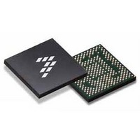
SC900841JVK Freescale Semiconductor, SC900841JVK Datasheet - Page 167

SC900841JVK
Manufacturer Part Number
SC900841JVK
Description
IC POWER MGT 338-MAPBGA
Manufacturer
Freescale Semiconductor
Specifications of SC900841JVK
Applications
PC's, PDA's
Operating Temperature
-40°C ~ 85°C
Mounting Type
Surface Mount
Package / Case
338-TBGA
Input Voltage
2.8 V to 4.4 V
Maximum Operating Temperature
+ 85 C
Minimum Operating Temperature
- 40 C
Lead Free Status / RoHS Status
Lead free / RoHS Compliant
Current - Supply
-
Voltage - Supply
-
Lead Free Status / Rohs Status
Lead free / RoHS Compliant
Available stocks
Company
Part Number
Manufacturer
Quantity
Price
Company:
Part Number:
SC900841JVK
Manufacturer:
Freescale Semiconductor
Quantity:
10 000
Company:
Part Number:
SC900841JVKR2
Manufacturer:
Freescale Semiconductor
Quantity:
10 000
- Current page: 167 of 192
- Download datasheet (8Mb)
Table 111. ADC Channel Selector/Configuration Structure and bit Description
Table 110. ADC Control Registers Structure and Bits Description
Analog Integrated Circuit Device Data
Freescale Semiconductor
ADEXGAIN17
ADEXGAIN18
ADEXGAIN19
ADEXGAIN20
ADEXGAIN21
Reserved
ADCHxH
ADCHxL
ADSELx
XPXMx
YPYMx
XMYPx
GAINx
Name
Reserved
Bits
6:0
2:0
7:3
4:0
7
5
6
7
7:4
7
0
1
2
3
7 MSBs of ADC result for Channel x
Gain bit for ADC channel x, x = 0 to 31
x0 = x1 (0-2.0 V input range)
x1 = x10 (0-200 mV input range)
3 LSBs of ADC result for Channel x
Reserved
ADC Channel to be read Selection bits
x00 = Channel 0
x01 = Channel 1
...
x1F = Channel 31
Turns on X+ and X- bias FETs, Refer to
x0 = FETS Off
x1 = FETS On
Turns on Y+ and Y- bias FETs, Refer to
x0 = FETS Off
x1 = FETS On
Turns on X- and Y+ bias FETs, Refer to
x0 = FETS Off
x1 = FETS On
Gain bit for ADC channel 17
x0 = x1 (0-2.0 V input range)
x1 = x10 (0-200 mV input range)
Gain bit for ADC channel 18
x0 = x1 (0-2.0 V input range)
x1 = x10 (0-200 mV input range)
Gain bit for ADC channel 19
x0 = x1 (0-2.0 V input range)
x1 = x10 (0-200 mV input range)
Gain bit for ADC channel 20
x0 = x1 (0-2.0 V input range)
x1 = x10 (0-200 mV input range)
Gain bit for ADC channel 21
x0 = x1 (0-2.0 V input range)
x1 = x10 (0-200 mV input range)
Reserved
ADCCNTL4 (ADDR 0X63 - R/W -DEFAULT VALUE: 0X00)
ADCADDRX (X = 0 TO 31)
ADCSNSxH (x = 0 to 31)
ADCSNSxL (x = 0 to 31)
Figure 76
Figure 76
Figure 76
Description
FUNCTIONAL DEVICE OPERATION
ADC SUBSYSTEM
900841
167
Related parts for SC900841JVK
Image
Part Number
Description
Manufacturer
Datasheet
Request
R
Part Number:
Description:
Manufacturer:
Freescale Semiconductor, Inc
Datasheet:
Part Number:
Description:
Manufacturer:
Freescale Semiconductor, Inc
Datasheet:
Part Number:
Description:
Manufacturer:
Freescale Semiconductor, Inc
Datasheet:
Part Number:
Description:
Manufacturer:
Freescale Semiconductor, Inc
Datasheet:
Part Number:
Description:
Manufacturer:
Freescale Semiconductor, Inc
Datasheet:
Part Number:
Description:
Manufacturer:
Freescale Semiconductor, Inc
Datasheet:
Part Number:
Description:
Manufacturer:
Freescale Semiconductor, Inc
Datasheet:
Part Number:
Description:
Manufacturer:
Freescale Semiconductor, Inc
Datasheet:
Part Number:
Description:
Manufacturer:
Freescale Semiconductor, Inc
Datasheet:
Part Number:
Description:
Manufacturer:
Freescale Semiconductor, Inc
Datasheet:
Part Number:
Description:
Manufacturer:
Freescale Semiconductor, Inc
Datasheet:
Part Number:
Description:
Manufacturer:
Freescale Semiconductor, Inc
Datasheet:
Part Number:
Description:
Manufacturer:
Freescale Semiconductor, Inc
Datasheet:
Part Number:
Description:
Manufacturer:
Freescale Semiconductor, Inc
Datasheet:
Part Number:
Description:
Manufacturer:
Freescale Semiconductor, Inc
Datasheet:


