OM13012,598 NXP Semiconductors, OM13012,598 Datasheet
OM13012,598
Specifications of OM13012,598
OM13012


Related parts for OM13012,598


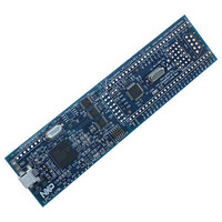
OM13012,598 Summary of contents
Page 1
LPC11Cx2/Cx4 32-bit ARM Cortex-M0 microcontroller; 16/32 kB flash SRAM; C_CAN Rev. 2 — 3 December 2010 1. General description The LPC11Cx2/Cx4 are an ARM Cortex-M0 based, low-cost 32-bit MCU family, designed for 8/16-bit microcontroller applications, offering performance, low ...
Page 2
... NXP Semiconductors Programmable WatchDog Timer (WDT). Analog peripherals: 10-bit ADC with input multiplexing among 8 pins. Serial interfaces: UART with fractional baud rate generation, internal FIFO, and RS-485 support. Two SPI controllers with SSP features and with FIFO and multi-protocol capabilities. ...
Page 3
... NXP Semiconductors 4. Ordering information Table 1. Ordering information Type number Package Name LPC11C12FBD48/301 LQFP48 LPC11C14FBD48/301 LQFP48 LPC11C22FBD48/301 LQFP48 LPC11C24FBD48/301 LQFP48 4.1 Ordering options Table 2. Ordering options Type number Flash LPC11C12FBD48/301 16 kB LPC11C14FBD48/301 32 kB LPC11C22FBD48/301 16 kB LPC11C24FBD48/301 32 kB LPC11CX2_CX4 Product data sheet Description LQFP48: plastic low profile quad flat package ...
Page 4
... NXP Semiconductors 5. Block diagram LPC11Cx2/Cx4 HIGH-SPEED GPIO ports GPIO PIO0/1/2/3 RXD TXD DTR, DSR, CTS, DCD, RI, RTS CT32B0_MAT[3:0] 32-bit COUNTER/TIMER 0 CT32B0_CAP0 CT32B1_MAT[3:0] 32-bit COUNTER/TIMER 1 CT32B1_CAP0 CT16B0_MAT[2:0] 16-bit COUNTER/TIMER 0 CT16B0_CAP0 (1) CT16B1_MAT[1:0] 16-bit COUNTER/TIMER 1 CT16B1_CAP0 CAN_TXD C_CAN (LPC11C12/C14) CAN_RXD CANL, CANH STB ON-CHIP TRANSCEIVER ...
Page 5
... NXP Semiconductors 6. Pinning information 6.1 Pinning PIO2_6 PIO2_0/DTR/SSEL1 RESET/PIO0_0 PIO0_1/CLKOUT/CT32B0_MAT2 V XTALIN XTALOUT V PIO1_8/CT16B1_CAP0 PIO0_2/SSEL0/CT16B0_CAP0 PIO2_7 PIO2_8 Fig 2. Pin configuration (LPC11C12/C14) LPC11CX2_CX4 Product data sheet LPC11C12FBD48/301 LPC11C14FBD48/301 All information provided in this document is subject to legal disclaimers. Rev. 2 — 3 December 2010 LPC11Cx2/Cx4 32-bit ARM Cortex-M0 microcontroller ...
Page 6
... NXP Semiconductors PIO2_6 PIO2_0/DTR/SSEL1 RESET/PIO0_0 PIO0_1/CLKOUT/CT32B0_MAT2 V XTALIN XTALOUT V PIO1_8/CT16B1_CAP0 PIO0_2/SSEL0/CT16B0_CAP0 PIO2_7 PIO2_8 Fig 3. Pin configuration (LPC11C22/C24) LPC11CX2_CX4 Product data sheet LPC11C22FBD48/301 LPC11C24FBD48/301 All information provided in this document is subject to legal disclaimers. Rev. 2 — 3 December 2010 LPC11Cx2/Cx4 32-bit ARM Cortex-M0 microcontroller 36 PIO3_0/DTR 35 R/PIO1_2/AD3/CT32B1_MAT1 ...
Page 7
... NXP Semiconductors 6.2 Pin description Table 3. LPC11C12/C14 pin description table Symbol Pin Start logic inputs PIO0_0 to PIO0_11 [2] RESET/PIO0_0 3 yes [3] PIO0_1/CLKOUT/ 4 yes CT32B0_MAT2 [3] PIO0_2/SSEL0/ 10 yes CT16B0_CAP0 [3] PIO0_3 14 yes [4] PIO0_4/SCL 15 yes [4] PIO0_5/SDA 16 yes [3] PIO0_6/SCK0 22 yes [3] PIO0_7/CTS 23 yes [3] PIO0_8/MISO0/ 27 yes CT16B0_MAT0 [3] PIO0_9/MOSI0/ 28 yes CT16B0_MAT1 ...
Page 8
... NXP Semiconductors Table 3. LPC11C12/C14 pin description table Symbol Pin Start logic inputs [5] R/PIO0_11/ 32 yes AD0/ CT32B0_MAT3 PIO1_0 to PIO1_11 [5] R/PIO1_0/AD1/ 33 yes CT32B1_CAP0 [5] R/PIO1_1/AD2 CT32B1_MAT0 [5] no R/PIO1_2/AD3/ 35 CT32B1_MAT1 [5] SWDIO/PIO1_3 AD4/ CT32B1_MAT2 [5] PIO1_4/AD5 CT32B1_MAT3/ WAKEUP [3] PIO1_5/RTS CT32B0_CAP0 [3] PIO1_6/RXD CT32B0_MAT0 LPC11CX2_CX4 Product data sheet Type ...
Page 9
... NXP Semiconductors Table 3. LPC11C12/C14 pin description table Symbol Pin Start logic inputs [3] PIO1_7/TXD CT32B0_MAT1 [3] PIO1_8 CT16B1_CAP0 [3] PIO1_9 CT16B1_MAT0 [5] PIO1_10/AD6 CT16B1_MAT1 [5] PIO1_11/AD7 42 no PIO2_0 to PIO2_11 [3] PIO2_0/DTR SSEL1 [3] PIO2_1/DSR/SCK1 13 no [3] PIO2_2/DCD MISO1 [3] PIO2_3/RI/MOSI1 38 no [3] PIO2_4 18 no [3] PIO2_5 21 no [3] PIO2_6 1 no [3] PIO2_7 11 no [3] PIO2_8 ...
Page 10
... NXP Semiconductors Table 3. LPC11C12/C14 pin description table Symbol Pin Start logic inputs [3] PIO3_0/DTR 36 no [3] PIO3_1/DSR 37 no [3] PIO3_2/DCD 43 no [3] PIO3_3/ [6] CAN_RXD 19 no [6] CAN_TXD [7] XTALIN 6 - [7] XTALOUT [1] Pin state at reset for default function Input Output internal pull-up enabled inactive, no pull-up/down enabled. [2] See Figure 26 for reset pad configuration ...
Page 11
... NXP Semiconductors Table 4. LPC11C22/C24 pin description table Symbol Pin Start logic inputs [3] PIO0_1/CLKOUT/ 4 yes CT32B0_MAT2 [3] PIO0_2/SSEL0/ 10 yes CT16B0_CAP0 [3] PIO0_3 14 yes [4] yes PIO0_4/SCL 15 [4] PIO0_5/SDA 16 yes [3] PIO0_6/SCK0 23 yes [3] PIO0_7/CTS 24 yes [3] PIO0_8/MISO0/ 27 yes CT16B0_MAT0 [3] PIO0_9/MOSI0/ 28 yes CT16B0_MAT1 [3] SWCLK/PIO0_10/ 29 yes SCK0/ CT16B0_MAT2 [5] R/PIO0_11/ 32 yes ...
Page 12
... NXP Semiconductors Table 4. LPC11C22/C24 pin description table Symbol Pin Start logic inputs [5] R/PIO1_0/AD1/ 33 yes CT32B1_CAP0 [5] R/PIO1_1/AD2 CT32B1_MAT0 [5] R/PIO1_2/AD3 CT32B1_MAT1 [5] SWDIO/PIO1_3 AD4/ CT32B1_MAT2 [5] PIO1_4/AD5 CT32B1_MAT3/ WAKEUP [3] PIO1_5/RTS CT32B0_CAP0 [3] PIO1_6/RXD CT32B0_MAT0 [3] PIO1_7/TXD CT32B0_MAT1 [3] PIO1_8 CT16B1_CAP0 [5] PIO1_10/AD6 CT16B1_MAT1 LPC11CX2_CX4 Product data sheet Type Reset ...
Page 13
... NXP Semiconductors Table 4. LPC11C22/C24 pin description table Symbol Pin Start logic inputs [5] PIO1_11/AD7 42 no PIO2_0 to PIO2_11 [3] PIO2_0/DTR SSEL1 [3] PIO2_1/DSR/SCK1 13 no [3] PIO2_2/DCD MISO1 [3] PIO2_3/RI/MOSI1 38 no [3] PIO2_6 1 no [3] PIO2_7 11 no [3] PIO2_8 12 no [3] PIO2_10 25 no [3] PIO2_11/SCK0 31 no PIO3_0 to PIO3_3 [3] PIO3_0/DTR 36 no [3] PIO3_1/DSR 37 no [3] PIO3_2/DCD ...
Page 14
... NXP Semiconductors Table 4. LPC11C22/C24 pin description table Symbol Pin Start logic inputs GND [7] XTALIN 6 - [7] XTALOUT [1] Pin state at reset for default function Input Output internal pull-up enabled inactive, no pull-up/down enabled. [2] See Figure 26 for reset pad configuration. RESET functionality is not available in Deep power-down mode. Use the WAKEUP pin to reset the chip and wake up from Deep power-down mode ...
Page 15
... NXP Semiconductors 7. Functional description 7.1 ARM Cortex-M0 processor The ARM Cortex- general purpose, 32-bit microprocessor, which offers high performance and very low power consumption. 7.2 On-chip flash program memory The LPC11Cx2/Cx4 contain 32 kB (LPC11C14/C24 (LPC11C12/C22) of on-chip flash program memory. 7.3 On-chip SRAM The LPC11Cx2/Cx4 contain a total on-chip static RAM data memory ...
Page 16
... NXP Semiconductors LPC11Cx2/Cx4 4 GB reserved private peripheral bus reserved AHB peripherals reserved APB peripherals 1 GB reserved 0.5 GB reserved 16 kB boot ROM reserved 8 kB SRAM reserved 32 kB on-chip flash (LPC11Cx4 on-chip flash (LPC11Cx2 Fig 4. LPC11Cx2/Cx4 memory map 7.5 Nested Vectored Interrupt Controller (NVIC) The Nested Vectored Interrupt Controller (NVIC integral part of the Cortex-M0 ...
Page 17
... NXP Semiconductors • Four programmable interrupt priority levels, with hardware priority level masking. • Software interrupt generation. 7.5.2 Interrupt sources Each peripheral device has one interrupt line connected to the NVIC but may have several interrupt flags. Individual interrupt flags may also represent more than one interrupt source ...
Page 18
... NXP Semiconductors Support for RS-485/9-bit mode allows both software address detection and automatic address detection using 9-bit mode. The UART includes a fractional baud rate generator. Standard baud rates such as 115200 Bd can be achieved with any crystal frequency above 2 MHz. 7.8.1 Features • ...
Page 19
... NXP Semiconductors receivers can operate in either master or slave mode, depending on whether the chip has to initiate a data transfer or is only addressed. The I controlled by more than one bus master connected to it. 7.10.1 Features • The C-bus interface also supports Fast-mode Plus with bit rates Mbit/s. ...
Page 20
... NXP Semiconductors – C_CAN status – CANopen object dictionary – CANopen SDO expedited communication – CANopen SDO segmented communication primitives – CANopen SDO fall-back handler • Flash ISP programming via C_CAN supported. 7.11.2 On-chip, high-speed CAN transceiver Remark: The on-chip CAN transceiver is available on parts LPC11C22/C24 only. ...
Page 21
... NXP Semiconductors to a permanent dominant state (blocking all network communications). The TXD dominant time-out timer is reset when the CAN_TXD signal is set HIGH. The TXD dominant time-out time also defines the minimum possible bit rate of 40 kbit/s. 7.12 10-bit ADC The LPC11Cx2/Cx4 contains one ADC. The ADC is a single 10-bit successive approximation ADC with eight channels ...
Page 22
... NXP Semiconductors 7.14 System tick timer The ARM Cortex-M0 includes a system tick timer (SYSTICK) that is intended to generate a dedicated SYSTICK exception at a fixed time interval (typically 10 ms). 7.15 Watchdog timer The purpose of the watchdog is to reset the microcontroller within a selectable time period. ...
Page 23
... NXP Semiconductors IRC oscillator watchdog oscillator IRC oscillator system oscillator SYSPLLCLKSEL (system PLL clock select) Fig 5. LPC11Cx2/Cx4 clock generation block diagram 7.16.1.1 Internal RC oscillator The IRC may be used as the clock source for the WDT, and/or as the clock that drives the PLL and subsequently the CPU. The nominal IRC frequency is 12 MHz. The IRC is trimmed accuracy over the entire voltage and temperature range ...
Page 24
... NXP Semiconductors 7.16.1.3 Watchdog oscillator The watchdog oscillator can be used as a clock source that directly drives the CPU, the watchdog timer, or the CLKOUT pin. The watchdog oscillator nominal frequency is programmable between 7.8 kHz and 1.7 MHz. The frequency spread over processing and temperature is ...
Page 25
... NXP Semiconductors 7.16.5.2 Deep-sleep mode In Deep-sleep mode, the chip is in Sleep mode, and in addition all analog blocks are shut down exception, the user has the option to keep the watchdog oscillator and the BOD circuit running for self-timed wake-up and BOD protection. Deep-sleep mode allows for additional power savings ...
Page 26
... NXP Semiconductors NVIC in order to cause a CPU interrupt; if not, software can monitor the signal by reading a dedicated status register. Four additional threshold levels can be selected to cause a forced reset of the chip. 7.17.4 Code security (Code Read Protection - CRP) This feature of the LPC11Cx2/Cx4 allows user to enable different levels of security in the system so that access to the on-chip flash and use of the Serial Wire Debugger (SWD) and In-System Programming (ISP) can be restricted ...
Page 27
... NXP Semiconductors The C_CAN ISP command handler uses the CANopen protocol and data organization method. C_CAN ISP commands have the same functionality as UART ISP commands. 7.17.6 APB interface The APB peripherals are located on one APB bus. 7.17.7 AHBLite The AHBLite connects the CPU bus of the ARM Cortex-M0 to the flash memory, the main static RAM, and the Boot ROM ...
Page 28
... NXP Semiconductors 8. Limiting values Table 5. Limiting values In accordance with the Absolute Maximum Rating System (IEC 60134). Symbol Parameter V supply voltage (core DD and external rail) V input voltage I I supply current DD I ground current SS I I/O latch-up current latch T storage temperature stg T maximum junction ...
Page 29
... NXP Semiconductors 9. Static characteristics Table 6. Static characteristics +85 C, unless otherwise specified. amb Symbol Parameter V supply voltage (core DD and external rail) I supply current DD Standard port pins, RESET I LOW-level input current HIGH-level input IH current I OFF-state output OZ current V input voltage I V output voltage ...
Page 30
... NXP Semiconductors Table 6. Static characteristics +85 C, unless otherwise specified. amb Symbol Parameter I HIGH-level output OH current I LOW-level output OL current I HIGH-level short-circuit OHS output current I LOW-level short-circuit OLS output current I pull-down current pd I pull-up current pu High-drive output pin (PIO0_7) I LOW-level input current V ...
Page 31
... NXP Semiconductors Table 6. Static characteristics +85 C, unless otherwise specified. amb Symbol Parameter I LOW-level output OL current I LOW-level short-circuit OLS output current I pull-down current pd I pull-up current C-bus pins (PIO0_4 and PIO0_5) V HIGH-level input IH voltage V LOW-level input voltage IL V hysteresis voltage ...
Page 32
... NXP Semiconductors [13] 3-state outputs go into 3-state mode in Deep power-down mode. [14] Allowed as long as the current limit does not exceed the maximum current allowed by the device. [15 9.1 ADC characteristics Table 7. ADC static characteristics +85 C unless otherwise specified; ADC frequency 4.5 MHz, V ...
Page 33
... NXP Semiconductors 1023 1022 1021 1020 1019 1018 7 code out offset error E O (1) Example of an actual transfer curve. (2) The ideal transfer curve. (3) Differential linearity error (E (4) Integral non-linearity (E L(adj) (5) Center of a step of the actual transfer curve. Fig 6. ADC characteristics LPC11CX2_CX4 Product data sheet ...
Page 34
... NXP Semiconductors 9.2 CAN on-chip, high-speed transceiver characteristics Table 8. Static characteristics = 40 C to +85 amb CC ground; positive currents flow into the IC. Also see Symbol Parameter Supply; pin VCC V supply voltage CC I supply current CC V undervoltage detection uvd(VCC) voltage on pin V CC I/O level adapter supply ...
Page 35
... NXP Semiconductors Table 8. Static characteristics = 40 C to +85 amb CC ground; positive currents flow into the IC. Also see Symbol Parameter I recessive output current O(rec) I leakage current L R input resistance i R input resistance deviation i R differential input resistance i(dif) C common-mode input ...
Page 36
... NXP Semiconductors 9.3 BOD static characteristics Table 10 amb Symbol V th [1] Interrupt levels are selected by writing the level value to the BOD control register BODCTRL, see LPC11Cx user manual. 9.4 Power consumption Power measurements in Active, Sleep, and Deep-sleep modes were performed under the following conditions (see LPC11Cx user manual): • ...
Page 37
... NXP Semiconductors (mA) (1) System oscillator and system PLL disabled; IRC enabled. (2) System oscillator and system PLL enabled; IRC disabled. Fig 7. (mA) (1) System oscillator and system PLL disabled; IRC enabled. (2) System oscillator and system PLL enabled; IRC disabled. Fig 8. LPC11CX2_CX4 Product data sheet ...
Page 38
... NXP Semiconductors (mA) (1) System oscillator and system PLL disabled; IRC enabled. (2) System oscillator and system PLL enabled; IRC disabled. Fig 9. (μA) Fig 10. Deep-sleep mode: Typical supply current I LPC11CX2_CX4 Product data sheet −40 −15 Conditions 3.3 V; sleep mode entered from flash; all peripherals disabled in the DD SYSAHBCLKCTRL register (SYSAHBCLKCTRL = 0x1F) ...
Page 39
... NXP Semiconductors (μA) Fig 11. Deep power-down mode: Typical supply current I LPC11CX2_CX4 Product data sheet 0 0.6 0.4 0.2 0 −40 −15 different supply voltages V DD All information provided in this document is subject to legal disclaimers. Rev. 2 — 3 December 2010 LPC11Cx2/Cx4 32-bit ARM Cortex-M0 microcontroller VDD = 3 ...
Page 40
... NXP Semiconductors 9.5 Peripheral power consumption The supply current per peripheral is measured as the difference in supply current between the peripheral block enabled and the peripheral block disabled in the SYSAHBCLKCFG and PDRUNCFG (for analog blocks) registers. All other blocks are disabled in both registers and no code is executed. Measured on a typical sample at T noted otherwise, the system oscillator and PLL are running in both measurements ...
Page 41
... NXP Semiconductors 9.6 Electrical pin characteristics V Fig 12. High-drive output: Typical HIGH-level output voltage V (mA) Fig 13. I LPC11CX2_CX4 Product data sheet 3 °C (V) 25 °C −40 °C 3.2 2.8 2 Conditions 3 pin PIO0_7. DD output current 0.2 Conditions 3 pins PIO0_4 and PIO0_5 C-bus pins (high current sink): Typical LOW-level output current I ...
Page 42
... NXP Semiconductors (mA) Fig 14. Typical LOW-level output current I V Fig 15. Typical HIGH-level output voltage V LPC11CX2_CX4 Product data sheet 0.2 Conditions 3.3 V; standard port pins and PIO0_7. DD 3 °C 25 °C 3.2 −40 °C 2.8 2 Conditions 3.3 V; standard port pins All information provided in this document is subject to legal disclaimers. ...
Page 43
... NXP Semiconductors (μA) Fig 16. Typical pull-up current I (μA) Fig 17. Typical pull-down current I LPC11CX2_CX4 Product data sheet −10 − °C 25 °C −40 °C −50 − Conditions 3.3 V; standard port pins. DD versus input voltage ° °C −40 ° Conditions 3.3 V; standard port pins. ...
Page 44
... NXP Semiconductors 10. Dynamic characteristics 10.1 Flash memory Table 12. amb Symbol N endu t ret prog [1] Number of program/erase cycles. [2] Programming times are given for writing 256 bytes from RAM to the flash. Data must be written to the flash in blocks of 256 bytes. 10.2 External clock Table 13. ...
Page 45
... NXP Semiconductors 10.3 Internal oscillators Table 14. amb Symbol f osc(RC) [1] Parameters are valid over operating temperature range unless otherwise specified. Typical ratings are not guaranteed. The values listed are at room temperature (25 C), nominal supply [2] voltages. (MHz) Fig 19. Internal RC oscillator frequency vs. temperature Table 15 ...
Page 46
... NXP Semiconductors 10.4 I/O pins Table 16. amb Symbol [1] Applies to standard port pins and RESET pin. 2 10.5 I C-bus Table 17. amb Symbol f SCL LOW t HIGH t HD;DAT t SU;DAT [1] See the I [2] Parameters are valid over operating temperature range unless otherwise specified. [3] tHD;DAT is the data hold time that is measured from the falling edge of SCL; applies to data in transmission and the acknowledge ...
Page 47
... NXP Semiconductors [6] The maximum t output stage t SDA and the SCL pins and the SDA/SCL bus lines without exceeding the maximum specified t [7] In Fast-mode Plus, fall time is specified the same for both output stage and bus timing. If series resistors are used, designers should allow for this when considering bus timing. ...
Page 48
... NXP Semiconductors Table 18. Dynamic characteristics of SPI pins in SPI mode Symbol Parameter t data set-up time DS t data hold time DH t data output valid time in SPI mode v(Q) t data output hold time in SPI mode h(Q) = (SSPCLKDIV SCR) CPSDVSR [1] T cy(clk) main clock frequency f ...
Page 49
... NXP Semiconductors SCK (CPOL = 0) SCK (CPOL = 1) Fig 22. SPI slave timing in SPI mode LPC11CX2_CX4 Product data sheet T cy(clk) MOSI DATA VALID t MISO DATA VALID MOSI DATA VALID t v(Q) MISO DATA VALID Pin names SCK, MISO, and MOSI refer to pins for both SPI peripherals, SPI0 and SPI1. ...
Page 50
... NXP Semiconductors 11. Application information 11.1 ADC usage notes The following guidelines show how to increase the performance of the ADC in a noisy environment beyond the ADC specifications listed in • The ADC input trace must be short and as close as possible to the LPC11Cx2/Cx4 chip. • The ADC input traces must be shielded from fast switching digital signals and noisy power supply lines. • ...
Page 51
... NXP Semiconductors Fig 24. Oscillator modes and models: oscillation mode of operation and external crystal Table 19. Fundamental oscillation frequency F 1 MHz - 5 MHz 5 MHz - 10 MHz 10 MHz - 15 MHz 15 MHz - 20 MHz Table 20. Fundamental oscillation frequency F 15 MHz - 20 MHz 20 MHz - 25 MHz 11.3 XTAL Printed Circuit Board (PCB) layout guidelines The crystal should be connected on the PCB as close as possible to the oscillator input and output pins of the chip ...
Page 52
... NXP Semiconductors order to keep the noise coupled in via the PCB as small as possible. Also parasitics should stay as small as possible. Values of C accordingly to the increase in parasitics of the PCB layout. 11.4 Standard I/O pad configuration Figure 25 • Digital output driver • Digital input: Pull-up enabled/disabled • ...
Page 53
... NXP Semiconductors 11.5 Reset pad configuration Fig 26. Reset pad configuration 11.6 C_CAN with external transceiver (LPC11C12/C14 only) Fig 27. Connecting the C_CAN to an external transceiver (LPC11C12/C14) LPC11CX2_CX4 Product data sheet reset GLITCH FILTER BAT CANH CANH TJF1051 CANL CANL All information provided in this document is subject to legal disclaimers. ...
Page 54
... NXP Semiconductors 11.7 C_CAN with on-chip, high-speed transceiver (LPC11C22/C24 only) Fig 28. Connecting the CAN high-speed transceiver to the CAN bus (LPC11C22/C24) LPC11CX2_CX4 Product data sheet CANH CANH CAN HIGH-SPEED TRANSCEIVER CANL CANL All information provided in this document is subject to legal disclaimers. Rev. 2 — 3 December 2010 ...
Page 55
... NXP Semiconductors 12. Package outline LQFP48: plastic low profile quad flat package; 48 leads; body 1 pin 1 index DIMENSIONS (mm are the original dimensions) A UNIT max. 0.20 1.45 1.6 mm 0.25 0.05 1.35 Note 1. Plastic or metal protrusions of 0.25 mm maximum per side are not included. OUTLINE VERSION ...
Page 56
... NXP Semiconductors 13. Abbreviations Table 21. Acronym ADC AHB APB API BOD CAN GPIO PLL RC SDO SPI SSI SSP UART LPC11CX2_CX4 Product data sheet Abbreviations Description Analog-to-Digital Converter Advanced High-performance Bus Advanced Peripheral Bus Application Programming Interface BrownOut Detection Controller Area Network General Purpose Input/Output ...
Page 57
... NXP Semiconductors 14. Revision history Table 22. Revision history Document ID Release date LPC11CX2_CX4 v.2 20101203 Modifications: LPC11C12_C14 v.1 20100921 LPC11CX2_CX4 Product data sheet Data sheet status Product data sheet • Parts LPC11C22 and LPC11C24 added. • Pin description for parts LPC11C22 and LPC11C24 added • ...
Page 58
... In no event shall NXP Semiconductors be liable for any indirect, incidental, punitive, special or consequential damages (including - without limitation - lost profits, lost savings, business interruption, costs related to the removal or ...
Page 59
... For sales office addresses, please send an email to: LPC11CX2_CX4 Product data sheet own risk, and (c) customer fully indemnifies NXP Semiconductors for any liability, damages or failed product claims resulting from customer design and use of the product for automotive applications beyond NXP Semiconductors’ ...
Page 60
... NXP Semiconductors 17. Contents 1 General description . . . . . . . . . . . . . . . . . . . . . . 1 2 Features and benefits . . . . . . . . . . . . . . . . . . . . 1 3 Applications . . . . . . . . . . . . . . . . . . . . . . . . . . . . 2 4 Ordering information . . . . . . . . . . . . . . . . . . . . . 3 4.1 Ordering options . . . . . . . . . . . . . . . . . . . . . . . . 3 5 Block diagram . . . . . . . . . . . . . . . . . . . . . . . . . . 4 6 Pinning information . . . . . . . . . . . . . . . . . . . . . . 5 6.1 Pinning . . . . . . . . . . . . . . . . . . . . . . . . . . . . . . . 5 6.2 Pin description . . . . . . . . . . . . . . . . . . . . . . . . . 7 7 Functional description . . . . . . . . . . . . . . . . . . 15 7.1 ARM Cortex-M0 processor . . . . . . . . . . . . . . . 15 7.2 On-chip flash program memory . . . . . . . . . . . 15 7.3 On-chip SRAM ...
Page 61
... NXP Semiconductors 14 Revision history . . . . . . . . . . . . . . . . . . . . . . . . 57 15 Legal information 15.1 Data sheet status . . . . . . . . . . . . . . . . . . . . . . 58 15.2 Definitions . . . . . . . . . . . . . . . . . . . . . . . . . . . . 58 15.3 Disclaimers . . . . . . . . . . . . . . . . . . . . . . . . . . . 58 15.4 Trademarks Contact information Contents . . . . . . . . . . . . . . . . . . . . . . . . . . . . . . 60 LPC11Cx2/Cx4 32-bit ARM Cortex-M0 microcontroller Please be aware that important notices concerning this document and the product(s) described herein, have been included in section ‘Legal information’. ...