AD2S99APZ Analog Devices Inc, AD2S99APZ Datasheet - Page 6
AD2S99APZ
Manufacturer Part Number
AD2S99APZ
Description
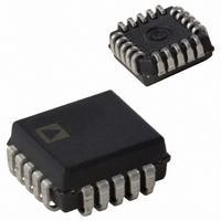
IC, PROG OSCILLATOR, 20KHZ, 5.25V, LCC20
Manufacturer
Analog Devices Inc
Type
Oscillator, Sinusoidalr
Datasheet
1.AD2S99APZ.pdf
(8 pages)
Specifications of AD2S99APZ
Supply Voltage Range
± 4.75V To ± 5.25V
Digital Ic Case Style
LCC
No. Of Pins
20
Operating Temperature Range
-40°C To +85°C
Frequency Max
20kHz
Termination Type
SMD
Frequency
20kHz
Voltage - Supply
±4.75 V ~ 5.25 V
Current - Supply
8mA
Operating Temperature
-40°C ~ 85°C
Package / Case
20-PLCC
Filter Terminals
SMD
Rohs Compliant
Yes
Accuracy
5
Lead Free Status / RoHS Status
Lead free / RoHS Compliant
Count
-
Lead Free Status / RoHS Status
Lead free / RoHS Compliant, Lead free / RoHS Compliant
Available stocks
Company
Part Number
Manufacturer
Quantity
Price
Company:

Part Number:
AD2S99APZ
Manufacturer:
AD
Quantity:
5 530
Company:
Part Number:
AD2S99APZ
Manufacturer:
AD
Quantity:
1 000
Company:
Part Number:
AD2S99APZ
Manufacturer:
Analog Devices Inc
Quantity:
135
Company:
Part Number:
AD2S99APZ
Manufacturer:
Analog Devices Inc
Quantity:
10 000
Part Number:
AD2S99APZ
Manufacturer:
ADI/亚德诺
Quantity:
20 000


AD2S99
AD2S99/AD2S82A TYPICAL CONFIGURATION
Figure 4 shows a typical circuit configuration for the AD2S99
Oscillator and the AD2S82A Resolver-to-Digital Converter.
The maximum level of the SIN and COS input signals to the
AD2S82A should be 2 V rms 10%. All the analog ground sig-
nals should be star connected to the AD2S82A AGND pin. If
shielded twisted pair cables are used for the resolver signals, the
shields should also be terminated at the AD2S82A AGND pin.
NC = NO CONNECT
DGND
SIN
COS
SIN
NC
NC
4
5
6
7
8
3
9
SEL1 = GND
SEL2 = V
F
OUT
(Not to Scale)
10
AD2S99
TOP VIEW
2
= 10kHz
11
1
50k
SS
–5V
12 13
20
Figure 4. AD2S99 and AD2S82A Example Configuration
SYNREF
0.1µF
19
4.7µF
COS
LOS
0.1µF
18
17
16
15
14
EXC
EXC
AGND
NC
NC
4.7µF
REF
+5V
10µF
+12V
RESOLVER
AGND
COS
0.1µF
SIN
MSB DB1
DGND
DIGITAL
OUTPUT
DB2
DB3
DB4
DB5
DB6
DB7
DB8
+V
SIN
DATA
–6–
NC
I/P
S
10
11
12
13
14
15
16
17
7
8
9
Coupling capacitor C3, and resistor to GND R3, between the
SYNREF output of the AD2S99 and the REF input pin of the
AD2S82A are optional. For additional information on selecting
component values for the AD2S82A, please refer to the
AD2S82A data sheet or the application note “Passive Compo-
nent Selection and Dynamic Modeling for the AD2S80 Series
Resolver-to-Digital Converters” (AN-266).
R3, C3 OPTIONAL
C3
18
6
19
5
R3
20
4
C1
R1
21
3
(Not to Scale)
AD2S82A
22
R2
2
TOP VIEW
23
VELOCITY
1
OUTPUT
R4
44
24
C2
0.1µF
R5
43
25
C4
C5
42
26
41
27
40
28
10µF
R6
39
38
37
36
35
34
33
32
31
30
29
+5V
0.1µF
–V
RC
BUSY
DATA LOAD
INHIBIT
NC
DIR
COMP
SC2
SC1
DIGITAL GND
S
–12V
AGND
0V
10µF
REV. B
Related parts for AD2S99APZ
Image
Part Number
Description
Manufacturer
Datasheet
Request
R

Part Number:
Description:
±1.7g Dual-Axis IMEMS Accelerometer Evaluation Board
Manufacturer:
Analog Devices Inc
Datasheet:

Part Number:
Description:
Inertial Sensor Evaluation System
Manufacturer:
Analog Devices Inc
Datasheet:
Part Number:
Description:
Manufacturer:
Analog Devices Inc
Datasheet:
Part Number:
Description:
Manufacturer:
Analog Devices Inc
Datasheet:
Part Number:
Description:
Manufacturer:
Analog Devices Inc
Datasheet:
Part Number:
Description:
Manufacturer:
Analog Devices Inc
Datasheet:
Part Number:
Description:
Manufacturer:
Analog Devices Inc
Datasheet:
Part Number:
Description:
Manufacturer:
Analog Devices Inc
Datasheet:
Part Number:
Description:
Manufacturer:
Analog Devices Inc
Datasheet:
Part Number:
Description:
Manufacturer:
Analog Devices Inc
Datasheet:
Part Number:
Description:
Manufacturer:
Analog Devices Inc
Datasheet:
Part Number:
Description:
Manufacturer:
Analog Devices Inc
Datasheet:
Part Number:
Description:
Manufacturer:
Analog Devices Inc
Datasheet: