DS90LV019TM National Semiconductor, DS90LV019TM Datasheet
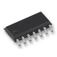
LVDS PHY TRANSCEIVER 155MBS, SOIC8

DS90LV019TM

Manufacturer Part Number
DS90LV019TM
Description
LVDS PHY TRANSCEIVER 155MBS, SOIC8
Manufacturer
National Semiconductor
Datasheet

Specifications of DS90LV019TM

Supply Voltage Range
3V To 3.6V, 4.5V To 5.5V
Digital Ic Case Style
SOIC
No. Of Pins
14
Operating Temperature Range
-40°C To +85°C
Svhc
No SVHC (15-Dec-2010)
Operating Temperature Max
85°C
Base Number
90
Data Rate
100Mbps
Rohs Compliant
Yes
Supply Current
12mA
Driver Case Style
TSSOP
Device Type
Driver / Receiver
Filter Terminals
SMD
Data Rate Max
100Mbps
Lead Free Status / RoHS Status
Lead free / RoHS Compliant

Available stocks

Company
Part Number
Manufacturer
Quantity
Price
Part Number:
DS90LV019TM
Manufacturer:
NS
Quantity:
545
Part Number:
DS90LV019TM
Manufacturer:
LATTICE
Quantity:
1
Part Number:
DS90LV019TM
Manufacturer:
MOT
Quantity:
60
Part Number:
DS90LV019TM
Manufacturer:
NS/国半
Quantity:
20 000
Company:
Part Number:
DS90LV019TM
Quantity:
7 000
Part Number:
DS90LV019TM/NOPB
Manufacturer:
TI
Quantity:
1 500
Part Number:
DS90LV019TM/NOPB
Manufacturer:
National Semiconductor
Quantity:
1 983
Part Number:
DS90LV019TMTC
Manufacturer:
national
Quantity:
246
Part Number:
DS90LV019TMTCX
Manufacturer:
NS/国半
Quantity:
20 000
Part Number:
DS90LV019TMX
Manufacturer:
NS/国半
Quantity:
20 000
© 2000 National Semiconductor Corporation
DS90LV019
3.3V or 5V LVDS Driver/Receiver
General Description
The DS90LV019 is a Driver/Receiver designed specifically
for the high speed low power point-to-point interconnect ap-
plications. The device operates from a single 3.3V or 5.0V
power supply and includes one differential line driver and
one receiver. The DS90LV019 features an independent
driver and receiver with TTL/CMOS compatibility (D
R
separate lines are provided (D
device also features a flow-through pin out which allows
easy PCB routing for short stubs between its pins and the
connector. The driver has 3.5 mA output loop current.
The driver translates between TTL levels (single-ended) to
Low Voltage Differential Signaling levels. This allows for high
speed operation, while consuming minimal power with re-
duced EMI. In addition, the differential signaling provides
common-mode noise rejection.
The receiver threshold is
mode range and translates the low swing differential levels
to standard (TTL/CMOS) levels.
Connection Diagram
Block Diagram
TRI-STATE
OUT
). The logic interface provides maximum flexibility as 4
®
is a registered trademark of National Semiconductor Corporation.
±
100 mV over a
IN
, DE, RE, and R
Order Number DS90LV019TM or DS90LV019TMTC
DS100053
See NS Package Number M14A or MTC14
±
1V common-
OUT
IN
). The
and
Features
n LVDS Signaling
n 3.3V or 5.0V operation
n Low power CMOS design
n Balanced Output Impedance
n Glitch free power up/down (Driver disabled)
n High Signaling Rate Capacity (above 100 Mbps)
n Ultra Low Power Dissipation
n
n
n Product offered in SOIC and TSSOP packages
n Flow-Through Pin Out
n Industrial Temperature Range Operation
DS100053-2
±
±
1V Common-Mode Range
100 mV Receiver Sensitivity
DS100053-1
www.national.com
August 2000

Related parts for DS90LV019TM

DS90LV019TM Summary of contents

Page 1

... Ultra Low Power Dissipation ). The OUT ± 1V Common-Mode Range n ± 100 mV Receiver Sensitivity n n Product offered in SOIC and TSSOP packages n Flow-Through Pin Out n Industrial Temperature Range Operation ± 1V common- DS100053-1 Order Number DS90LV019TM or DS90LV019TMTC See NS Package Number M14A or MTC14 DS100053-2 DS100053 August 2000 www.national.com ...

Page 2

... Absolute Maximum Ratings If Military/Aerospace specified devices are required, please contact the National Semiconductor Sales Office/ Distributors for availability and specifications. Supply Voltage V CC Enable Input Voltage (DE, RE) Driver Input Voltage ( Receiver Output Voltage (R ) OUT ± Driver Output Voltage (DO ) ± Receiver Input Voltage (RI ...

Page 3

DC Electrical Characteristics T = −40˚C to +85˚C unless otherwise noted Symbol Parameter DIFFERENTIAL DRIVER CHARACTERISTICS V Output Differential Voltage Magnitude Change Offset Voltage OS V Offset Magnitude Change OS I TRI-STATE ...

Page 4

AC Electrical Characteristics ± −40˚C to +85˚ 3. Symbol Parameter DRIVER TIMING REQUIREMENTS t Disable Time High to Z PHZ t Disable Time Low to Z PLZ t Enable Time Z to High PZH ...

Page 5

Test Circuits and Timing Waveforms FIGURE 2. Differential Driver Propagation Delay and Transition Test Circuit FIGURE 3. Differential Driver Propagation and Transition Time Waveforms FIGURE 1. Differential Driver DC Test Circuit FIGURE 4. Driver TRI-STATE Delay Test Circuit 5 DS100053-3 ...

Page 6

Test Circuits and Timing Waveforms FIGURE 6. Receiver Propagation Delay and Transition Time Test Circuit FIGURE 7. Receiver Propagation Delay and Transition Time Waveforms www.national.com (Continued) FIGURE 5. Driver TRI-STATE Delay Waveforms FIGURE 8. Receiver TRI-STATE Delay Test Circuit 6 ...

Page 7

Test Circuits and Timing Waveforms FIGURE 9. Receiver TRI-STATE Delay Waveforms TRI-STATE Delay Waveforms Typical Application Diagram Applications Information The DS90LV019 has two control pins, which allows the de- vice to operate as a driver, a receiver or both driver ...

Page 8

Applications Information • Balanced cables (e.g., twisted pair) are usually better than unbalanced cables (ribbon cable, simple coax) for noise reduction and signal quality. < • For cable distances 0.5m, most cables can be made to work effectively. For distances ...

Page 9

... Physical Dimensions inches (millimeters) unless otherwise noted Order Number DS90LV019TM NS Package Number M14A 9 www.national.com ...

Page 10

... National does not assume any responsibility for use of any circuitry described, no circuit patent licenses are implied and National reserves the right at any time without notice to change said circuitry and specifications. inches (millimeters) unless otherwise noted (Continued) Order Number DS90LV019TMTC NS Package Number MTC14 2 ...

Related keywords