DS3695ATM National Semiconductor, DS3695ATM Datasheet
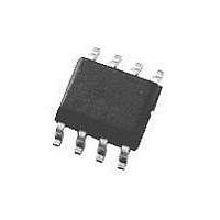
IC, RS422/RS485 TRANSCEIVER, 5V, NSOIC-8

DS3695ATM

Manufacturer Part Number
DS3695ATM
Description
IC, RS422/RS485 TRANSCEIVER, 5V, NSOIC-8
Manufacturer
National Semiconductor
Datasheet

Specifications of DS3695ATM

Device Type
Transceiver
Ic Interface Type
RS422, RS485
No. Of Drivers
1
Supply Voltage Range
4.75V To 5.25V
Driver Case Style
SOIC
No. Of Pins
8
Interface Type
RS422, RS485
Operating Temperature Range
-40°C To +85°C
Svhc
No SVHC
Rohs Compliant
Yes
Lead Free Status / RoHS Status
Contains lead / RoHS non-compliant

Available stocks

Company
Part Number
Manufacturer
Quantity
Price
Part Number:
DS3695ATM
Manufacturer:
NS
Quantity:
6
Part Number:
DS3695ATM
Manufacturer:
NS
Quantity:
2 580
Company:
Part Number:
DS3695ATM
Quantity:
193
Part Number:
DS3695ATM/NOPB
Manufacturer:
NS
Quantity:
1 068
Part Number:
DS3695ATMX
Manufacturer:
NEC
Quantity:
3 000
Part Number:
DS3695ATMX
Manufacturer:
NS
Quantity:
1 000
Part Number:
DS3695ATMX
Manufacturer:
NS/国半
Quantity:
20 000
Part Number:
DS3695ATMX/NOPB
Manufacturer:
OKI
Quantity:
6 230
© 2004 National Semiconductor Corporation
DS3695A/DS3695AT/DS3696A
Multipoint RS485/RS422 Transceivers
General Description
The DS3695A and DS3696A are high speed differential
TRI-STATE
quirements of EIA standard RS485 with extended common
mode range (+12V to −7V), for multipoint data transmission.
In addition they are compatible with requirements of RS-422.
The driver and receiver outputs feature TRI-STATE capabil-
ity. The driver outputs remain in TRI-STATE over the entire
common mode range of +12V to −7V. Bus faults that cause
excessive power dissipation within the device trigger a ther-
mal shutdown circuit, which forces the driver outputs into the
high impedance state. The DS3696A provides an output pin
(TS) which reports the thermal shutdown of the device. TS is
an “open collector” pin with an internal 10 kΩ pull-up resistor.
This allows the TS outputs of several devices to be wire
OR-ed.
Both AC and DC specifications are guaranteed over the 0˚C
to 70˚C temperature and 4.75V to 5.25V supply voltage
range.
Connection and Logic Diagram
TS was LF (Line Fault) on previous datasheets, TS goes low upon thermal shutdown.
TRI-STATE
®
is a registered trademark of National Semiconductor Corporation.
®
bus/line transceivers designed to meet the re-
Order Number DS3695AM, DS3695ATM or DS3696AM
DS005272
Molded Package, Small Outline (M)
See NS Package Number M08A
Top View
Top View
Features
n Meets EIA standard RS485 for multipoint bus
n 10 ns driver propagation delays (typical)
n Single +5V supply
n −7V to +12V bus common mode range permits
n Thermal shutdown protection
n High impedance to bus with driver in TRI-STATE or with
n Combined impedance of a driver output and receiver
n 70 mV typical receiver hysteresis
n Available in SOIC packaging
transmission and is compatible with RS-422
ground difference between devices on the bus
power off, over the entire common mode range allows
the unused devices on the bus to be powered down
input is less than one RS485 unit load, allowing up to 32
transceivers on the bus
00527201
00527202
February 1996
www.national.com
±
7V

Related parts for DS3695ATM

DS3695ATM Summary of contents

Page 1

... Both AC and DC specifications are guaranteed over the 0˚C to 70˚C temperature and 4.75V to 5.25V supply voltage range. Connection and Logic Diagram TS was LF (Line Fault) on previous datasheets, TS goes low upon thermal shutdown. Order Number DS3695AM, DS3695ATM or DS3696AM TRI-STATE ® registered trademark of National Semiconductor Corporation. © 2004 National Semiconductor Corporation ...

Page 2

... Storage Temp. Range Lead Temp. (Soldering 4 seconds) Recommended Operating 7V Conditions 7V 7V Supply Voltage, V +15V/−10V Bus Voltage +15V/−10V Operating Free Air Temp. (T 5.5V Commercial (DS3695AM) Industrial (DS3695ATM) Commercial (DS3696AM) 630 mW (Note 4) (Notes 2, 3) Conditions 50Ω; (RS-422) (Note 27Ω; (RS-485 27Ω DI − ...

Page 3

Note 2: All currents into device pins are positive; all currents out of device pins are negative. All voltages are referenced to device ground unless otherwise specified. Note 3: All typicals are given for and T CC ...

Page 4

AC Test Circuits and Switching Waveforms Differential input voltage may be realized by grounding RI and pulsing RI between +2.5V and −2.5V FIGURE 2. Receiver Input-to-Output Propagation Delay Timing FIGURE 3. Receiver Enable/Disable Propagation Delay Timing Unless otherwise specified the ...

Page 5

AC Test Circuits and Switching Waveforms t and t are measured to the respective 50% points. t PLH PHL FIGURE 5. Driver Input-to-Output Propagation Delay Timing (Single-Ended) FIGURE 6. Driver Enable/Disable Propagation Delay Timing FIGURE 7. Driver Differential Transition Timing ...

Page 6

Function Tables DS3695A/DS3696A Transmitting Inputs DS3695A/DS3696A Receiving — Don’t care condition Z — High impedance state Fault — Improper ...

Page 7

... Physical Dimensions inches (millimeters) unless otherwise noted Order Number DS3695AM, DS3695ATM or DS3696AM National does not assume any responsibility for use of any circuitry described, no circuit patent licenses are implied and National reserves the right at any time without notice to change said circuitry and specifications. ...

Related keywords