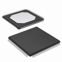
XC2C384-10TQG144C Xilinx Inc, XC2C384-10TQG144C Datasheet - Page 9

XC2C384-10TQG144C
Manufacturer Part Number
XC2C384-10TQG144C
Description
IC, CPLD, 384 MACROCELL, 7.1NS, TQFP-144
Manufacturer
Xilinx Inc
Series
CoolRunner IIr
Specifications of XC2C384-10TQG144C
No. Of Macrocells
384
No. Of I/o's
118
Propagation Delay
7.1ns
Global Clock Setup Time
3.3ns
Frequency
125MHz
Supply Voltage Range
1.7V To 1.9V
Programmable Type
In System Programmable
Delay Time Tpd(1) Max
9.2ns
Voltage Supply - Internal
1.7 V ~ 1.9 V
Number Of Logic Elements/blocks
24
Number Of Macrocells
384
Number Of Gates
9000
Number Of I /o
118
Operating Temperature
0°C ~ 70°C
Mounting Type
Surface Mount
Package / Case
144-TQFP, 144-VQFP
Features
JTAG
Voltage
1.8V
Memory Type
CMOS
Rohs Compliant
Yes
Lead Free Status / RoHS Status
Lead free / RoHS Compliant
Number Of Logic Elements/cells
-
Lead Free Status / RoHS Status
Lead free / RoHS Compliant, Lead free / RoHS Compliant
Other names
122-1406
Available stocks
Company
Part Number
Manufacturer
Quantity
Price
Company:
Part Number:
XC2C384-10TQG144C
Manufacturer:
XILINX
Quantity:
214
Company:
Part Number:
XC2C384-10TQG144C
Manufacturer:
XILINX
Quantity:
455
Company:
Part Number:
XC2C384-10TQG144C
Manufacturer:
Xilinx Inc
Quantity:
10 000
Additional Clock Options: Division,
DualEDGE, and CoolCLOCK
Clock Divider
A clock divider circuit has been included in the
CoolRunner-II CPLD architecture to divide one externally
supplied global clock by standard values. The allowable val-
ues for the division are 2, 4, 6, 8, 10, 12, 14, and 16 (see
Figure
resulting clock produced has a 50% duty cycle for all possi-
ble divisions. The output of the clock divider is on global
routing. If the clock divider is used, the undivided clock is
available internally. If the undivided clock is required inter-
nally it is input through a separate clock pin.
The clock divider circuit encompasses a synchronous reset
(CDRST) to guarantee no spurious clocks can carry
through on to the global clock nets. When the CDRST signal
is asserted, the clock divider output is disabled after the cur-
rent cycle. When the CDRST signal is deasserted the clock
divider output becomes active upon the first edge of GCK2.
The CDRST pin functions as a reset pin regardless of which
CLK_DIV primitive is used. If a clock divider is used in the
design, the CDRST pin is reserved and if it is driven High
the clock divider is reset. If a reset port of a clock divider is
not used, it is tied Low on the board. The clock divider circuit
includes an active High synchronous reset, referred to as
CDRST.
The CoolRunner-II CPLD clock divider includes a built-in
delay circuit. With the delay feature enabled, the output of
the clock divider is delayed for one full count cycle. When
used, the clock divider does not output a rising clock edge
until after the divider reaches the delay value. The delay fea-
ture is either enabled or disabled upon configuration.
Xilinx Synthesis Technology (XST) allows a clock divider
component to be instantiated directly in the HDL source
code. See
Verilog, and ABEL.
DS090 (v3.1) September 11, 2008
Product Specification
8). This capability is supplied on the GCK2 pin. The
XAPP378
R
for instantiation examples in VHDL,
CDRST
GCK2
Figure 8: Clock Division Circuitry for GCK2
Clock
In
www.xilinx.com
CDRST
÷10
÷12
÷14
÷16
÷2
÷4
÷6
÷8
DualEDGE
Each macrocell has the ability to double its input clock
switching frequency.
with the DualEDGE option (doubled clock) at each macro-
cell. The source to double can be a control term clock, a
product term clock or one of the available global clocks. The
ability to switch on both clock edges, also known as dual
edge triggered (DET), is vital for a number of synchronous
memory interface applications as well as certain double
data rate I/O applications.
CoolRunner-II CPLD DET registers can be used for logic
functions that include shift registers, counters, comparators,
and state machines. Designers must evaluate the desired
performance of the CPLD logic to determine use of DET
registers.
The DET register can be inferred in any ABEL, HDL, or
schematic design. A designer can infer a single-edge trig-
gered (SET) register in any HDL design. The DET register is
available with all macrocells in all devices of the
CoolRunner-II family.
CoolCLOCK
In addition to the DualEDGE flip-flop, power savings can
occur by combining the clock division circuitry with the
DualEDGE circuitry. This capability is called CoolCLOCK
and is designed to reduce clocking power within the CPLD.
Because the clock net can be an appreciable power drain,
the clock power can be reduced by driving the net at half fre-
quency, then doubling the clock rate using DualEDGE trig-
gering at the macrocells.
is created by internal clock cascading with the divider and
DualEDGE flip-flop working together.
GCK2 is the only clock network that can be divided, the
CoolCLOCK feature is only available on GCK2. The Cool-
CLOCK feature can be implemented by assigning an
attribute to an input clock. The CoolCLOCK attribute
replaces the need to instantiate the clock divider and infer
DET registers. The CoolCLOCK feature is available on
CoolRunner-II 128 macrocell devices and larger. See
XAPP378
for more detail.
DS090_08_121201
Figure 9
Figure 10
CoolRunner-II CPLD Family
shows the macrocell flip-flop
shows how CoolCLOCK
9


